VOL. 7, NO. 12, DECEMBER 2012
ISSN 1819-6608
ARPN Journal of Engineering and Applied Sciences
©2006-2012 Asian Research Publishing Network (ARPN). All rights reserved.
www.arpnjournals.com
SEVEN-LEVEL THREE PHASE CASCADED H-BRIDGE INVERTER
WITH A SINGLE DC SOURCE
1
T. Porselvi1 and Ranganath Muthu2
Sri Sairam Engineering College, Chennai, India
2
SSN College of Engineering, Chennai, India
E-Mail: tporselvi@yahoo.com
ABSTRACT
Multi level inverters (MLIs) have been attractive for high power applications. Among the various MLIs, the
Cascaded H-Bridge inverter is promising for grid connected wind power and photovoltaic applications. This paper
compares three types of MLIs namely the Neutral Point Clamped MLI, the Flying Capacitor MLI, and the Cascaded HBridge MLI. In addition, the Cascaded H-Bridge MLI with a single DC source is presented. These MLIs are simulated in
MATLAB using multi-carrier sine pulse width modulation (MCPWM) technique. Simulated output voltages and currents
for an RL load are shown for the four configurations and compared based on the total harmonic distortion (THD). Results
obtained show the applicability of the Cascaded H-Bridge inverter with a single DC source for grid connected wind power
applications.
Keywords: cascaded H-bridge inverter (CHB), multi carrier pulse width modulation (MCPWM), neutral point clamped inverter (NPC),
flying capacitor inverter (FLC), total harmonic distortion (THD).
1. INTRODUCTION
MLIs are becoming increasingly popular for their
high voltage operating capability, high power capability
and reduced EMI effects. MLIs have three or more voltage
levels; have lower total harmonic distortion (THD) and
less switching losses compared to the classical inverters.
There have been various designs for MLIs including the
following:
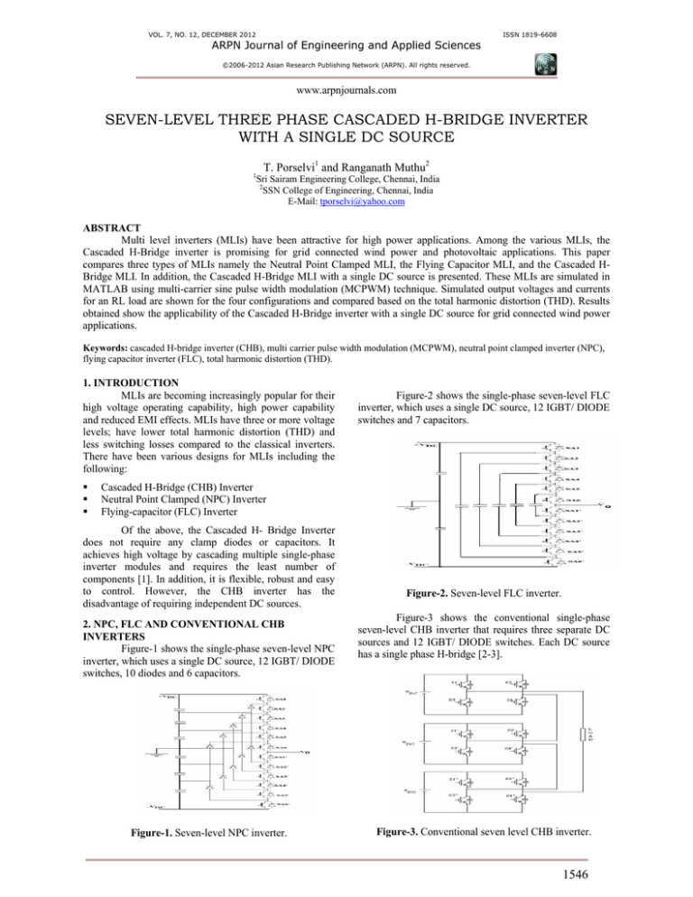
Figure-2 shows the single-phase seven-level FLC
inverter, which uses a single DC source, 12 IGBT/ DIODE
switches and 7 capacitors.
Cascaded H-Bridge (CHB) Inverter
Neutral Point Clamped (NPC) Inverter
Flying-capacitor (FLC) Inverter
Of the above, the Cascaded H- Bridge Inverter
does not require any clamp diodes or capacitors. It
achieves high voltage by cascading multiple single-phase
inverter modules and requires the least number of
components [1]. In addition, it is flexible, robust and easy
to control. However, the CHB inverter has the
disadvantage of requiring independent DC sources.
2. NPC, FLC AND CONVENTIONAL CHB
INVERTERS
Figure-1 shows the single-phase seven-level NPC
inverter, which uses a single DC source, 12 IGBT/ DIODE
switches, 10 diodes and 6 capacitors.
Figure-1. Seven-level NPC inverter.
Figure-2. Seven-level FLC inverter.
Figure-3 shows the conventional single-phase
seven-level CHB inverter that requires three separate DC
sources and 12 IGBT/ DIODE switches. Each DC source
has a single phase H-bridge [2-3].
Figure-3. Conventional seven level CHB inverter.
1546
VOL. 7, NO. 12, DECEMBER 2012
ISSN 1819-6608
ARPN Journal of Engineering and Applied Sciences
©2006-2012 Asian Research Publishing Network (ARPN). All rights reserved.
www.arpnjournals.com
3. MULTI CARRIER PWM
The most popular control technique used in MLIs
is the sinusoidal or “sub harmonic” natural pulse width
modulation (PWM) method. Its popularity is due to its
simplicity and to the good results it guarantees at all
operating conditions, including “over-modulation,” which
allows the first harmonic. It can be used for any MLI and
can be easily implemented. For an m-level inverter, m-1
carrier (triangular) waves with same amplitude and
frequency are required. The frequency modulation index,
which is the ratio of the carrier frequency to the
modulating signal frequency, is expressed by equation (1).
mf =
f cr
fm
(1)
Where, f m is the frequency of the modulating signal and
f cr is the frequency of the carrier waves. The amplitude
modulation index ma is defined by equation (2).
ma =
Where,
vm
vcr (m − 1)
(2)
Figure-4. PD modulation scheme for the seven-level
inverter.
MLIs are simulated for a star connected RL load
of 50+j7.53 Ω/phase. Figures 5 and 6 show the output
voltage and output current waveforms of the three-phase
seven-level NPC inverter. Figures 7 and 8 show the output
voltage and output current waveforms of the three-phase
seven-level FLC inverter. Figures 9 and 10 show the
output voltage and output current waveforms of the
three-phase seven-level CHB inverter with separate DC
sources.
vm is the peak value of the modulating wave and
vcr is the peak value of each carrier wave. Four carrier
PWM strategies, available in literature, with different
phase relations are [4-7]:
a)
b)
c)
d)
Phase Disposition (PD)
Phase Opposition Disposition (POD)
Alternate Phase Opposition Disposition (APOD)
Phase Shift (PS).
In this paper, PD modulation scheme is used for
pulse generation because it provides the lowest harmonic
distortion for line voltages [8].
Figure-5. Simulated output voltage of the NPC inverter.
4. SIMULATION USING MATLAB
Seven-level three-phase NPC, FLC and
conventional CHB MLIs are simulated with MATLAB for
an RL load. In PD technique, for an m level inverter, m-1
carrier waves are used which are in phase with each other.
These carrier waves are arranged to have vertical shifts.
Hence, for a seven-level inverter six carrier waves are
used to generate the switching pulses. These six carrier
waves are compared with a reference to obtain the
switching pulses. The PD scheme is shown in Figure-4.
Figure-6. Simulated output current of the NPC inverter.
1547
VOL. 7, NO. 12, DECEMBER 2012
ISSN 1819-6608
ARPN Journal of Engineering and Applied Sciences
©2006-2012 Asian Research Publishing Network (ARPN). All rights reserved.
www.arpnjournals.com
Figure-10. Simulated output current of the traditional
CHB inverter.
Figure-7. Simulated output voltage of the FLC inverter.
5. COMPARISON OF THE THDs
The FFT analysis obtained by simulating MLIs
are shown for the three configurations. Figures 11 and 12
respectively show the FFT analysis for the phase ‘a’
output voltage and output current for the NPC inverter.
Figures 13 and 14 respectively show the FFT analysis of
the phase ‘a’ output voltage and output current for the
FLC inverter. Figures 15 and 16 respectively show the
FFT analysis of the phase ‘a’ output voltage and output
current for the conventional CHB inverter.
Figure-8. Simulated output current of the FLC inverter.
Figure-11. FFT analysis of the output voltage of the NPC
inverter.
Figure-9. Simulated voltage of the traditional CHB
inverter.
Figure-12. FFT analysis of the output current of the NPC
inverter.
1548
VOL. 7, NO. 12, DECEMBER 2012
ISSN 1819-6608
ARPN Journal of Engineering and Applied Sciences
©2006-2012 Asian Research Publishing Network (ARPN). All rights reserved.
www.arpnjournals.com
respectively. The THD for four cycles of the output
current of NPC, FLC, and traditional CHB are 2%,
10.37%, 2.13%, respectively. Figure-17 shows the voltage
and current THDs for all the three inverters.
30.00%
25.00%
Figure-13. FFT analysis of the output voltage of the NPC
inverter.
20.00%
Voltage THD
15.00%
Current THD
10.00%
5.00%
0.00%
NPC inverter
Figure-14. FFT analysis of the output current of the FLC
inverter.
Figure-15. FFT analysis of the output voltage of the
conventional CHB inverter.
FLC Inverter
Traditional CHB Inverter
Figure-17. Voltage and current THDs for the NPC, FLC,
and CHB inverters.
From the simulated waveforms, it is seen that for
high power applications, CHB inverter is better suited as
its fundamental output voltages and currents are high. In
addition, the CHB inverter requires less number of
components compared to the NPC and the FLC inverters.
However, the CHB inverter has the disadvantage of
requiring separate DC sources for each level, which
increases the cost of the inverter. This disadvantage is not
present in the proposed CHB MLI as it uses only a single
DC source.
The simulation time, for four cycles of output, for
the three MLI configurations, vary between 1.5 s and
2.5 s, and is given in the Table-1. It can be seen that
simulation time for the CHB MLI of 1.75 s is comparable
to the least simulation time taken by the FLC MLI, which is
1.5 s.
Table-1. Simulation time for four cycles of output for the
three inverters.
Type of
inverter
Simulation
time in
seconds (s)
Figure-16. FFT analysis of the output current of the
traditional CHB inverter.
From Figures 11-16, it can be seen that the THD
for four cycles of the output voltage for the NPC, FLC,
and traditional CHB are 9.61%, 28.34%, and 9.52%,
NPC
MLI
FLC
MLI
CHB MLI
2.5
1.5
1.75
6. CHB MLI WITH A SINGLE DC SOURCE
Figure-18 shows the proposed single-phase
seven-level CHB MLI that uses a single DC source. The
output of the inverter is connected through transformers to
the load. The inverter uses three transformers per phase,
the secondary of each transformer being connected in
series. The load is connected across the series connected
secondary of the transformer [9-11].
1549
VOL. 7, NO. 12, DECEMBER 2012
ISSN 1819-6608
ARPN Journal of Engineering and Applied Sciences
©2006-2012 Asian Research Publishing Network (ARPN). All rights reserved.
www.arpnjournals.com
Figure-21. FFT analysis of the output voltage of the
proposed CHB inverter.
Figure-18. Seven-level CHB inverter with a single DC
Source.
The proposed seven-level three-phase CHB
inverter is simulated in MATLAB. Output voltage and
current waveforms are shown in Figures 19 and 20,
respectively.
Figure-22. FFT analysis of the output current of the
proposed CHB inverter.
Figures 23-34 show the switch currents and
switch voltages for 12 switches of one leg (phase) of the
proposed CHB inverter.
Figure-19. Simulated output voltages of the proposed
CHB inverter.
Figure-23. Switch current and voltage for S1.
Figure-20. Simulated output currents of the proposed
CHB inverter.
The FFT analysis of the output voltage and the
output current, obtained by simulation of the proposed
CHB inverter, is shown in Figures 21 and 22, respectively.
Figure-24. Switch current and voltage for S2.
1550
VOL. 7, NO. 12, DECEMBER 2012
ISSN 1819-6608
ARPN Journal of Engineering and Applied Sciences
©2006-2012 Asian Research Publishing Network (ARPN). All rights reserved.
www.arpnjournals.com
Figure-25. Switch current and voltage for S3.
Figure-29. Switch current and voltage for S3’.
Figure-26. Switch current and voltage for S4.
Figure-30. Switch current and voltage for S4’.
Figure-27. Switch current and voltage for S1’.
Figure-31. Switch current and voltage for S1”.
Figure-28. Switch current and voltage for S2’.
Figure-32. Switch current and voltage for S2”.
1551
VOL. 7, NO. 12, DECEMBER 2012
ISSN 1819-6608
ARPN Journal of Engineering and Applied Sciences
©2006-2012 Asian Research Publishing Network (ARPN). All rights reserved.
www.arpnjournals.com
Z n is the per phase load impedance given by equation (6)
and
φn is the power factor angle given by equation (7).
Z n = ( R 2 + (nωL) 2
φn = tan −1 (
Figure-33. Switch current and voltage for S3”.
(6)
nωL
)
R
(7)
The rms value of the phase current I a is given
by equation (8).
∞
Ia =
Figure-34. Switch current and voltage for S4”.
7. OUTPUT POWER CALCULATION
The Fourier series expansion of the phase voltage
of the CHB inverter is given by equation (3) [12].
Where
4VDC 3
[∑ cos(nα j )]sin( nωt )
nπ j =1
α
(3)
is the conduction angle and n = 1, 5, 7, etc.
The Fourier series expansion of the phase current,
which is also the line current for the star connected load, is
given by equation (4).
ia =
4VDC 3
[∑ cos(nα j )] sin( nωt − φn )
nπZ n j =1
(4)
The equation (4) can be rewritten as given by
equation (5).
3
ia = I n [∑ cos(nα j )] sin( nωt − φn )
j =1
Where I n =
4VDC
nπZ n
n =1
2
n
(8)
2
The output power is given by equation (10)
Figure-21 shows that the THD of the output
voltage of the proposed CHB inverter is 9.65% and
Figure-22 shows that the THD of the output current of the
proposed CHB inverter is 2.11%. The voltage THD of the
proposed inverter is slightly higher than that of the
conventional CHB inverter and the current THD of the
proposed CHB inverter is slightly lower than that of the
conventional CHB inverter. The proposed CHB may be
considered better as it costs less due to the requirement of
only one DC source, with performance comparable to the
conventional CHB inverter.
van =
∑I
(5)
Pout = 3I a2 R
(9)
For the conventional CHB inverter, the rms value
of the phase current is 8.28 A. The output power is given
by:
Pout = 3 * 8.28 2 * 50
= 10284 W
For the proposed CHB inverter, the rms value of
the phase current is found to be 8.27 A. Hence, the output
power is given by:
Pout = 3 * 8.27 2 * 50
= 10259 W
8. COMPARISON OF CHB MLI HAVING
SEPARATE DC SOURCES WITH CHB MLI
HAVING A SINGLE DC SOURCE
The two CHB inverters are simulated in
MATLAB with PD modulation with a star connected RL
load of 50+j7.53 Ω/phase. The output voltage, output
current and FFT analysis of voltage and current
waveforms of the CHB inverter with separate DC sources
were shown in the Figures 9, 10, 15 and 16 respectively.
Figures 19-21 show the output voltage, output current, and
FFT analysis of voltage and current of CHB with a single
DC source.
Table-2 shows the comparison of the proposed
CHB inverter with the conventional MLI. From Table-2, it
can be seen that THD values and power output of the CHB
MLI are comparable with the conventional one. It requires
one DC source, which reduces the cost of the proposed
CHB inverter.
1552
VOL. 7, NO. 12, DECEMBER 2012
ISSN 1819-6608
ARPN Journal of Engineering and Applied Sciences
©2006-2012 Asian Research Publishing Network (ARPN). All rights reserved.
www.arpnjournals.com
9. PARAMETERS FOR PROPOSED CHB
Input DC Voltage VDC = 200 V
Load Impedance/phase = 50+j7.53 Ω
IGBT/Diode voltage/current rating = 400 V/15A
Transformer rating = 200V/200V, 15A/15A
Table-2. Comparison of the conventional and the proposed CHBs.
Parameters
No. of DC sources
required
Number of IGBT/Diode
pairs
Voltage THD
Conventional CHB
MLI
Proposed CHB
MLI
Nine DC sources
One DC source
36
36
9.52 %
9.65 %
Current THD
2.13 %
2.11 %
Output power
10284 W
10259 W
US $ 5,500
US $ 3,600
400 V
400 V
15 A
15 A
Cost
Voltage rating of power
switches
Current rating of power
switches
10. CONCLUSIONS
The simulation of three Multi-level Inverters
(MLIs) namely the Neutral Point Clamped (NPC), the
Flying Capacitor (FLC) and the Cascaded H-Bridge
(CHB) is presented in this paper. These inverters are
simulated in MATLAB using multi-carrier sine pulse
width modulation (MCPWM) technique. The simulated
output voltage and current waveforms for an RL load are
shown for the three configurations and the total harmonic
distortion (THD) is compared. For high power
applications, CHB inverter is better suited as its
fundamental output voltages and currents are high. In
addition, the CHB inverter requires less number of
components compared to the NPC and the FLC inverters.
However, the CHB inverter has the disadvantage of
requiring separate DC sources for each level, which
increases the cost of the inverter.
The proposed Cascaded H-Bridge with a single
DC source is simulated in MATLAB using multi-carrier
sine pulse width modulation (MCPWM) technique. The
simulated output voltage and current waveforms, FFT
analysis and switching voltages and currents for an RL
load are shown for the proposed Cascaded H-Bridge with
a single DC source. The total harmonic distortion (THD),
output power and the cost for the two CHB Inverter
configurations are compared. The proposed CHB inverter
does not require separate DC sources and hence the cost of
the system is lesser. In addition, this system eliminates the
possibility of short circuit of the DC sources, which may
occur in the conventional CHB inverter.
REFERENCES
[1] Hong Zheng, Baohua Zhang and Lingkui Chen. 2010.
Carrier Overlapping-switching Frequency optional
PWM Method for Cascaded Multilevel Inverter. In:
International Conference on Electrical and Control
Engineering. 25-27 June. pp. 3450-3453.
[2] Peng F. Z., Lai J., McKeever J. W. and VanCoevering
J. 1996. A multilevel voltage-source inverter with
separate DC sources for static var generation. In:
IEEE Transactions on Industry Applications. 32(5):
1130-1138.
[3] Manjrekar M., Steimer P. K. and Lipo T. 2000.
Hybrid multilevel power conversion system: A
competitive solution for high-power applications. In:
IEEE Transactions on Industry Applications. 36(3):
834-84.
[4] Urmila B and Subbarayudu D. 2010. Multi level
Inverter: A Comparative Study of Pulse Width
Modulation Techniques. In: International Journal of
Scientific and Engineering research. 1(3): 2-5.
[5] Ilhami Colak, Ersan Kabalci and Ramazan Bayindir.
2011. Review of multilevel voltage source inverter
topologies and control schemes. In: Interna Journal on
Energy Conversion and Management. 52(2): 11141128.
[6] Wanjekeche T., V.Nicolae D. and Jimoh A.A. 2009.
Realization of a Nine - Level Cascaded NPC/ H-
1553
VOL. 7, NO. 12, DECEMBER 2012
ISSN 1819-6608
ARPN Journal of Engineering and Applied Sciences
©2006-2012 Asian Research Publishing Network (ARPN). All rights reserved.
www.arpnjournals.com
Bridge PWM Inverter using Phase-Shifted Carrier
PWM Technique. In: The International Conference on
Electrical Engineering, Hong Kong. 18-20 March.
pp. 1-6.
[7] McGrath B.P and Holmes D.G. 2002. Multicarrier
PWM Strategies for Multilevel Inverters. In: IEEE
Transaction on Industrial Electronics. 49(4): 858-867.
[8] Govindaraju C. and Baskaran K. 2009. Optimized
Hybrid Phase Disposition PWM Control Method for
Multilevel Inverter. In: International Journal of
Recent Trends in Engineering. 1(3): 129-134.
[9] Sung Geun Song, Feel Soon Kang and Sung-Jun Park.
2009. Cascaded Multilevel Inverter Employing ThreePhase Transformers and Single DC Input. In: IEEE
Transaction on Industrial Electronics. 56(6): 20052014.
[10] Suresh Y. and Panda A.K. 2010. Performance of
Cascade Multilevel H-Bridge Inverter with Single DC
Source by Employing Low Frequency Three Phase
Transformers. In: IECON- 36th Annual Conference of
IEEE Industrial Electronics Society. November 7-10,
Pheonix, AZ, USA. pp. 1981-1986.
[11] M. R. Banaei, E. Salary, R. Alizadeh and H.
Khounjahan 2012, Reduction of Components in
Cascaded Transformer Multilevel Inverter Using Two
DC Sources. In: Journal of Electrical Engineering and
Technology, 7(4), pp. 538-545.
[12] Zhong
Du, Leon M. Tolbert, John N.
Chiasson and Burak Özpineci. 2006. A
Cascaded Multilevel Inverter using Single
DC Source. In: Applied Power Electronics
Conference and Exposition, Semicond. Power
Electron. Center, North Carolina State Univ., Raleigh,
NC, USA. 19-20 March 2006. pp. 426-430.
1554
