JEOL JXA-8200 Superprobe: Electron Microscopy Techniques
advertisement
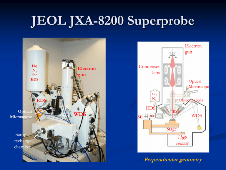
JEOL JXA-8200 Superprobe Electron gun Liq N2 for EDS Electron gun Condenser lens Optical Microscope Liq N2 EDS Optical Microscope EDS WDS Objective lens BSE SE WDS Stage Sample exchange chamber High vacuum Perpendicular geometry Back-scattered electron detector Top view of specimen Compositional and topographic imaging with BSE A+B Compositional mode A-B Topographic mode Secondary electrons Specimen electrons mobilized by electron beam through inelastic scattering • Secondary electrons have lower energy compared to backscattered electrons • (useful in studying surface topography) Secondary electron detector Side view of specimen Secondary electron imaging -ve Faraday cage bias less SE +ve Faraday cage bias more SE less topographic contrast better topographic contrast Cathodoluminescence Light generated from sample through electron beam interaction Band gap energy, Egap, is a property of the semiconductor Trace impurities change Egap by adding additional energy states in the band gap Cathodoluminescence detector JXA-733 Optical microscope light turned off Front view Side view Photomultiplier for secondary electron imaging is used as CL detector Optical arrangement is the same as for the optical microscope Cathodoluminescence spectrometer Optical microscope camera (not used) Optical microscope light (turned off) JXA-8200 Optical spectrometer Integrated CL and X-ray spectrometry Intensity CL spectrum Energy Scatter plot 3 band CL map 3 element X-ray map CL wavelength band may be correlated with an element Wavelength Dispersive Spectrometer (WDS) WDS WDS crystal detector WDS Analyzing crystal Flipping motor Bragg’s Law q = angle of diffraction d = lattice spacing nl = 2d sin q = path length ABC n = order of reflection (any integer) First and second order reflections Same element n=1 q1 n=2 q2 D A F C B E 1l = 2d sinq1 =ABC 2l = 2d sinq2 =DEF path DEF = 2* path ABC Diffraction angle l1 Different elements l2 (Element 2) (Element 1) q1 nl1 = 2d sinq1 q2 nl2 = 2d sinq2 Diffraction angle changes with wavelength being diffracted (for the same order of reflection, n) WDS Analyzing crystals with different “d” spacings Name LDEC STE LDE1 TAP PET LIF 2d (Å) 98 100.4 59.8 25.8 8.742 4.028 Type Ni/C Multi-layer Pb stearate W/Si Multi-layer Thallium acid phthalate Pentaerythritol Lithium fluoride Elements usually analyzed B-O (K), optimized for C analysis B-O (K), optimized for C analysis C-F (K), optimized for O analysis Na-P (K); Cu-Zr (L); Sm-Au (M) S-Mn (K); Nb-Pm (L); Hg-U (M) Ti-Rb (K); Ba-U (L) WDS detector: Proportional counter Count rate depends on bias and gas used Tungsten collection wire set at 1-3 kV bias Flow counter: 90% Ar +10% CH4 (P-10); poly-propylene window Sealed counter: Xe or Kr; Be window Bias in proportional counter best count rate Counting efficiency of gas Heavy elements Light elements WDS signal processing Single channel analyzer (SCA) and pulse height analysis (PHA) window baseline Only pulses in this voltage interval are counted WDS Focusing geometry angle of diffraction take-off angle L = nl .R/d Curved diffracting crystals Johansson type bending curvature: 2R polished and ground to R R Johan type only bent to 2R, not ground FWHM of fully focusing Johansson-type crystal ~10 eV Some defocusing in Johan-type, but resolution is not compromised Defocusing in beam-rastered WDS X-ray maps WDS: changing the angle of diffraction or, n2l1 = 2d sin q2 L2 = n2l1.R/d Theoretical and actual limits of spectrometer movement 2R ≤ L ≤ 0 EPMA: Quantitative analysis procedure Sample preparation Qualitative analysis with EDS Standard intensity measurement (calibration) Measurement of X-ray intensities in the specimen Data reduction through matrix corrections Sample preparation Sample cut and mounted in epoxy Polished first with coarse SiC paper, then with alumina grit slurry (final size: ≤0.25 mm) 1 Washed with water in ultrasonic cleaner 2 Dried with blow duster and air Carbon coated 3 1: diamond paste or colloidal silica for some samples; dry polishing paper for water-soluble samples 2: ethanol may be used sparingly; cleaned with blow duster and cloth for samples that dissolve in water 3: for insulators; if standards are coated, however, all samples must be coated Sample prep: carbon coating Sample chamber (bell jar) MIT OpenCourseWare http://ocw.mit.edu 12.119 Analytical Techniques for Studying Environmental and Geologic Samples Spring 2011 For information about citing these materials or our Terms of Use, visit: http://ocw.mit.edu/terms.
