Document 13436408
advertisement
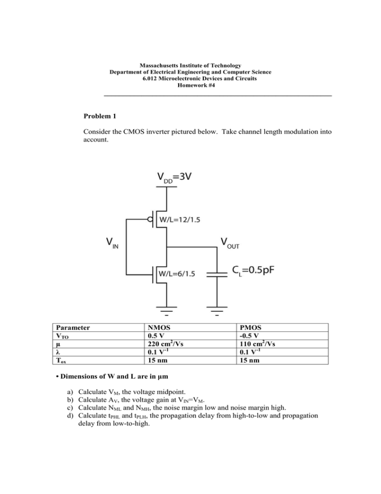
Massachusetts Institute of Technology Department of Electrical Engineering and Computer Science 6.012 Microelectronic Devices and Circuits Homework #4 _____________________________________________________________ Problem 1 Consider the CMOS inverter pictured below. Take channel length modulation into account. Parameter VTO µ λ Tox NMOS 0.5 V 220 cm2/Vs 0.1 V-1 15 nm PMOS -0.5 V 110 cm2/Vs 0.1 V-1 15 nm • Dimensions of W and L are in µm a) b) c) d) Calculate VM, the voltage midpoint. Calculate AV, the voltage gain at VIN=VM. Calculate NML and NMH, the noise margin low and noise margin high. Calculate tPHL and tPLH, the propagation delay from high­to­low and propagation delay from low­to­high. Problem 2 We will now use the following SPICE model and compare our hand calculations from Problem 1 with simulated results. .MODEL N15 NMOS LEVEL=1 VT0=0.5 TOX=1.5e­8 U0=220 LAMBDA=1.0e­1 +GAMMA=0.6 CJ=1e­4 CJSW=5e­10 PB=0.95 .MODEL P15 PMOS LEVEL=1 VT0=­0.5 TOX=1.5e­8 U0=110 LAMBDA=1.0e­1 +GAMMA=0.6 CJ=3e­4 CJSW=3.5e­10 PB=0.9 a) Use the DC sweep on the input voltage to simulate transfer characteristics using SPICE. Compare VM, AV, NML, NMH, with the calculated results. b) Use the Pulse input to simulate an input waveform shown below using SPICE. Compare tPHL and tPLH with your hand calculations. Problem 3 Consider the circuit below, which consists of an NMOS device and PMOS current source load. a) Calculate the width of the PMOS device so its saturation current is 50µA. b) Calculate VM, VOH, VOL. Remember, for hand calculations we assume VOH=VMAX, and VOL=VMIN. c) Calculate the voltage gain of this circuit, when VIN=VM. d) Calculate VOUT when VIN=3. MIT OpenCourseWare http://ocw.mit.edu 6.012 Microelectronic Devices and Circuits Spring 2009 For information about citing these materials or our Terms of Use, visit: http://ocw.mit.edu/terms.
