Using an FPGA to Control the Protection of National
advertisement
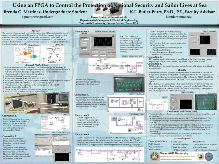
Using an FPGA to Control the Protection of National Security and Sailor Lives at Sea Brenda G. Martinez, Undergraduate Student bgmartinez@gmail.com K.L. Butler-Purry, Ph.D., P.E., Faculty Advisor klbutler@tamu.edu Power System Automation Lab Department of Computer & Electrical Engineering Texas A&M University, College Station, Texas, USA Abstract The purpose of this research is to interface a real-time (RT) simulation of a power system using field-programmable gate array (FPGA) technology that serves as a controller, using the following software: MATLAB/Simulink® , LabVIEW® 8.0, LabVIEW FPGA®, PharLAP ETS®, and National Instrument’s® (NI) Simulation Interface Toolkit® (SIT). Several connection phases need to be implemented to show that this integration is feasible. Flow Chart Connection 3. Real-Time Target VI Front Panel DAQ card produces a continuous analog output waveform using DAQmx Tasks. Specified number of samples are buffered and then continuously generated from device’s on-board memory. Project Concept Real-Time Target VI Block Panel Host VI Front Panel Host VI monitors the nominal voltage coming into the FPGA to make sure that the correct voltage is being read in and displays a digital waveform of the digital output from FPGA. There are two different ways of monitoring the digital output: 1. Using the DIO variables through the FPGA Read/Write tool. 2. Using DMA to directly read from the on-board FPGA memory. Connection 7. DO module sends out the control signal back to the DAQ card as a voltage. Digital high ranges from 4.3V-5V. Digital low ranges from .02V-.4V. Connection 8. Research Methodology Hardware was evaluated and purchased. The following steps are necessary in implementing the project concept of sending out a physical measurement from a real-time simulation, having it compared to a user controlled threshold, and returning a control signal back to the simulation. 1. Use MATLAB/Simulink® to create a signal. 2. SIT® to map between MATLAB® and LabVIEW®. 3. 6229 Data Acquisition (DAQ) card to produce the real analog output (AO) signal. 4. Analog Input (AI) 9215 Module to read in the analog signal. 5. FPGA to compare the amplitude of the analog signal to a threshold. 6. Monitor threshold with Host PC. 7. Digital output (DO) 9401 module to send out control signal. 8. 6229 DAQ card to receive the digital input (DI) signal. Hardware Configuration DAQ card receives control signal as a digital input, which is then sent back to the simulation. Results Oscilloscope Oscilloscope displaying physical voltage signal being produced by the DAQ card. Connection 4. • Connections 1-6 were successfully implemented with the use of various VIs. A signal was properly produced by the DAQ card from the RT target and the FPGA received an accurate transmission. The code on the FPGA was able to compare against a threshold and the Host VI was able to monitor the control signal. • The VI created for Connections 1 & 2 was not able to produce a physical sine wave using the DAQ card due to some errors with invalid tasks. There is an issue with a physical channel on the DAQ board being empty or not present. The following example VI though did work. SIT® Created VI FPGA VI Block Panel Oscilloscope Host Analog input module reads in the binary value that correlates to the voltage being read in through the AI Module. Loop rate serves as a delay between sample readings. Model Conclusions and Future Work Connection 1. Model Custom trigger on FPGA compares the analog input binary read with the binary value of a nominal voltage value set on the host VI. MATLAB/Simulink® models a sine wave. The Real-Time Workshop® builds a .DLL file of the sine wave that LabVIEW® can then use with real-time targets (CompactRio, PC, etc.) SIT ® Connection Manager Connection 2. SIT® Connection Manager Model and Host: Configures Execution Host and model locations. Mappings: Creates a bridge between variables in MATLAB/ Simulink® and LabVIEW®. Hardware I/O: Configures DAQ card to send and receive specified signals from simulation. Connection 5. FPGA VI Block Panel Connection 6. Host VI references the FPGA, runs the FPGA VI bit file that is already on the target, reads/writes to the variables, sets the loop rate at which the FPGA is sampling, converts the nominal voltage threshold value to a binary value, and when Host VI is stopped, sends an interrupt that stops the FPGA VI as well. Host VI Block Panel • Connections between hardware and computer systems were not straight forward as predicted. • Noted issues in recovering the waveform on the FPGA/host system and DO module not producing control signals are currently being worked on jointly with NI®. • LabVIEW 8.0® is not functioning correctly with the .dll builds of the Simulink® models using SimPowerSystems, although older versions have been known to work. Little SIT® testing with MATLAB® SimPowerSystems has been done previously. • More testing is necessary with SIT® and Simulink®, with updated MATLAB® versions to ensure proper measurements in real time. Acknowledgments •Fabian Marcel Uriarte Ph.D. Student •Ayo Akinnikawe M.Sc. Student •Andy Deck NI® Field Engineer •Travis Ferguson NI® Field Engineer •Efosa Ojomo NI® Applications Engineer •Steven Strahan NI® Applications Engineer
