CHIPS & NANOTECHNOLOGY
advertisement

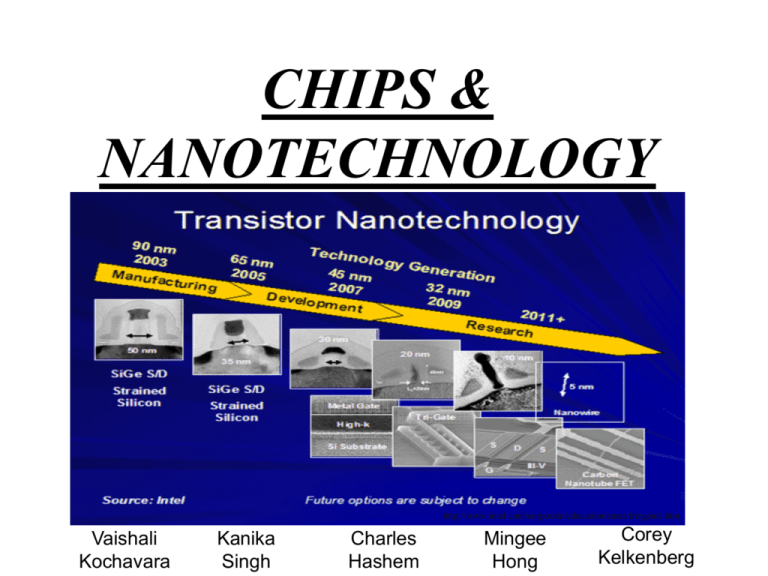
CHIPS & NANOTECHNOLOGY http://www.intel.com/corporate/education/emea/irc/goals.htm Vaishali Kochavara Kanika Singh Charles Hashem Mingee Hong Corey Kelkenberg How chips are made 1.Thermal Oxidation 2. Patterning 3. Etching 4. Doping 5. Final step http://www.appliedmaterials.com/investors/annual_report_1999/how_chips_are_made.html http://www.sematech.org/corporate/news/mfgproc/mfgproc.htm#steps1_2 Thermal Oxidation • Silicon Wafer chip making base on the silicon wafer. This can be made from large, cylindrical silicon crystals. Polishing it, and start chip making • Epitaxial Silicon for enhancing chip making, extremely pure silicon crystal layer grown on some wafers • Dielectric Deposition Using Chemical Vapor Deposition (CVD) technology, an insulating material called dielectric is deposited on the wafer surface, being grown and deposited in later steps Patterning http://www.appliedmaterials.com/investors/annual_report_1999/how_chips_are_made.html http://www.sematech.org/corporate/news/mfgproc/mfgproc.htm#steps1_2 • Photolithography Photo lithography is process used to make multiple layers of circuit pattern on the chip. wafer surface is deposited a light-sensitive chemical. It is repeated many times as each layer of the chip is built. Reticle Inspection systems help ensure that the image of the circuit pattern used by the photolithography system is defect-free. Etching • Etching removes selected material from the chip surface to create the device structures. http://www.appliedmaterials.com/investors/annual_report_1999/how_chips_are_made.html http://www.sematech.org/corporate/news/mfgproc/mfgproc.htm#steps1_2 Doping • • Ion Implantation shoots section of silicon with charged atoms accelerates “dopant” materials to a high velocity and shoots section of silicon and change the conductivity of the film. Rapid Thermal Processing (RTP) subjects the wafer to a very brief, intense burst of heat that can go from room temperature to 1000°C in seconds. This technology is used to change the characteristics of the deposited film. Final Step • Final Chip After processing, the chip is covered with a plastic or ceramic material to seal it tightly from the atmosphere. http://www.appliedmaterials.com/investors/annual_report_1999/how_chips_are_made.html http://www.sematech.org/corporate/news/mfgproc/mfgproc.htm#steps1_2 Moore’s Law – An Industry Driver Moore’s Law - Background -Gordon E. Moore, Co-Founder of Intel. • Law: -Moore’s Law deals with the growth of integrated circuits, primarily transistors, with a respect to minimum • component cost. -According to Moore’s Law the complexity of and integrated circuit will double about every 18 months but will cost the same to produce as the earlier model. • • Moore’s Law - Challenges • Moore’s Law faces many challenges put forth by the onset of nano-scale processing • Challenges include: – Transistors will soon be reaching the size of single atoms, a fundamental barrier that will be hard to overcome. – Thermal design needed to effectively handle the massive amount of dissipated power as chips become more and more powerful – The ability to fabricate gate terminals on single atom sized transistors that are still able to control the ON/OFF behavior of a chip. – Be able to solve all of these challenges WHILE reducing the overall cost of the entire system. Source: http://en.wikipedia.org/wiki/Moores_law Moore’s Law began as just an observation or an educated guess, but as time went on and the original predictions turned into reality, Moore’s Law became the “target” of semiconductor and chip manufacturers. These manufacturers believed that their competitors would be able to make the technological advances predicted by Moore so they set their goals accordingly. This proved to be a monumental engineering task, but Moore’s Law has held up since 1965 It may not hold up for long though due to some fundamental Challenges. Intel chip specifications – Pentium/MMX (circa 1993) to Pentium D “EE” (circa 2006) Source: http://www.tomshardware.com/2005/11/21/the_mother_of_all_cpu_charts_2005/page21.html The Growth of Moore’s Law • As more and more transistors are put onto a chip, as a chip gains more cores, larger cache sizes, and faster bus speeds, resulting in more calculations/second. • 100Ghz – Chips are NOT possible. – Moore’s Law is not based on chip operating frequencies, it is instead based on how much useful date can be calculated per second and how can we make this chip at the lowest possible price. We can expect 5ghz. • Moore’s Law will live on. – In the form of [(Processing Power)/Second]/Cost. Meaning that chip core speeds will slow down, but the amount of useful data that a chip can calculate per second for a certain minimum “cost” will continue to increase in accordance to Moore’s Law. Source: http://en.wikipedia.org/wiki/Moores_law The Future of Moore’s Law • As of Q1 of 2006 chip design manufacturers (AMD, INTEL, APPLE) have mass-produced chips on the 90nm scale in 64 bit, dual core, and 64 bit dual core. • Following the general trend of Moore’s Law a few of the companies (Intel, AMD) have begun to produce multiple cored, 64 bit chips, on the 65 nm scale • These companies are expected to come out with chips on the 45, 30, and possibly even smaller chip sizes in accordance with Moore’s Law. Intel is overcoming challenges! To meet the challenge of power loss Intel has been advancing a variety of novel power-saving techniques: • New process technologies, such as 65 nanometer (nm) • New transistor structures and materials, including strained silicon, tri-gate transistors • Innovative approaches to circuit and micro architecture design • New multi-core architectures • Advanced packaging materials • Improvements to system components • Software optimization techniques Bias : By dynamically adjusting the voltage applied to the body of a transistor (bias), one can manipulate the threshold voltage—the voltage at which the transistor turns on. Having localized control of the bias voltage enables the designer to make tradeoffs between the circuit performance and power it consumes. This capability can be used to reduce leakage during periods of inactivity or to increase performance during peak use. Dynamic Sleep Transistor is another innovative Intel technique that involves adding a transistor in series with the power supply that can be turned off when a block of logic circuitry is in idle mode, thus reducing leakage. http://www.intel.com/technology/silicon/power/chipdesign.htm http://www.intel.com/technology/silicon/power/index.htm THE 65NM CHIP • Intel's 65-nanometer (nm) process technology is the world's most advanced chip-manufacturing technology, and will enable future chips with increased capabilities and performance. Intel is at least a year ahead of the rest of the industry in shipping products based on 65nm process technology, in volume. The 65nm process features leading-edge transistor technology, unmatched by competition. • • Their leading-edge transistor technologies include: Second generation strained silicon with 10-15 percent improved drive current for improved performance 1.2nm gate oxide and 35nm gates for improved performance NiSi for low resistance cap on gates and source-drains Lower interconnect capacitance through low-k carbon doped oxide dielectric and 0.7x line length scaling providing increased performance and lower power • • • • Intel has initiated commercial production and revenue shipments of dual-core microprocessors based on the 65nm process technology on 300mm wafers, which enables cost-effective, high-volume manufacturing of multi-core microprocessors and other advanced products. Intel's 65nm technology roughly doubles transistor density compared to the 90nm chip. http://www.intel.com/technology/silicon/65nm_technology.htm http://www.intel.com/technology/silicon/si08042.htm More on 65 nm chip • Intel has integrated power saving features into the 65nm process technology which are critical to delivering power-efficient computing and communications products. Intel's 65nm transistors have a reduced gate length of 35 nm and a gate oxide thickness of 1.2 nm, which combine to provide improved performance and reduced gate capacitance. The reduced gate capacitance ultimately lowers a chip's active power. The new process also integrates eight copper interconnect layers and uses a "low-k" dielectric material that increases the signal speed inside the chip and reduces chip power consumption. • Sleep transistors" implemented in the 65nm SRAM shut off the current flow to large blocks of the SRAM when they are not being utilized, eliminating a significant source of power consumption on a chip. This is especially beneficial for battery-powered devices, like laptops. In addition, Intel now has an ultra-low-power 65nm process technology under development that will deliver power savings on mobile platforms and small-form-factor devices. This process addresses three types of transistor leakage: sub-threshold leakage, junction leakage and gate oxide leakage. The result is that the total leakage is reduced by roughly 1000 times from Intel's standard process while maintaining about 50 percent of the drive current. The benefits of reduced transistor leakage are lower power and increased battery life. http://www.intel.com/technology/silicon/si08042.htm http://www.intel.com/technology/silicon/65nm_technology.htm 45 NM CHIP- expected in 2007 Intel has produced what are believed to be the industry's first fully functional static random access memory (SRAM) chips using 45-nanometer (nm) process technology, in accordance with Moore’s Law. The 45nm process enables chip circuitry with higher performance-per-watt than the most advanced processes in production today. In the future, using the 45nm process will allow us to make chips with twice as many transistors in a given area. Intel's 45nm process technology will allow more energy efficient chips for mobile devices and increased opportunities for building smaller, more-powerful platforms. Part of the reason for this is, in comparison to the 65nm process, the new technology will provide twice the transistor density for smaller chips or increased transistor count & there will be a 20% improvement in transistor switching speed with a five-fold reduction in transistor current leakage benefiting battery life for mobile devices, making it possible to build smaller chips, thus smaller, more-powerful products. The 45nm SRAM chip has more than 1 billion transistors. 32 nm chip—expected in 2009 There is research going on also for the development of 32 nm sized chips. Intel plans to use extreme ultra-violet (EUV) lithography in the future which uses a series of mirrors to direct light with a wavelength of 13.5 nm to print exceptionally small features—elements as small as 32 nm and beyond. http://www.intel.com/pressroom/archive/releases/20060125comp.htm http://www.intel.com/technology/silicon/new_45nm_silicon.htm http://www.intel.com/technology/silicon/65nm_technology.htm


