ENGR-45_Lab-01a_MOSFET-Fabrication
advertisement
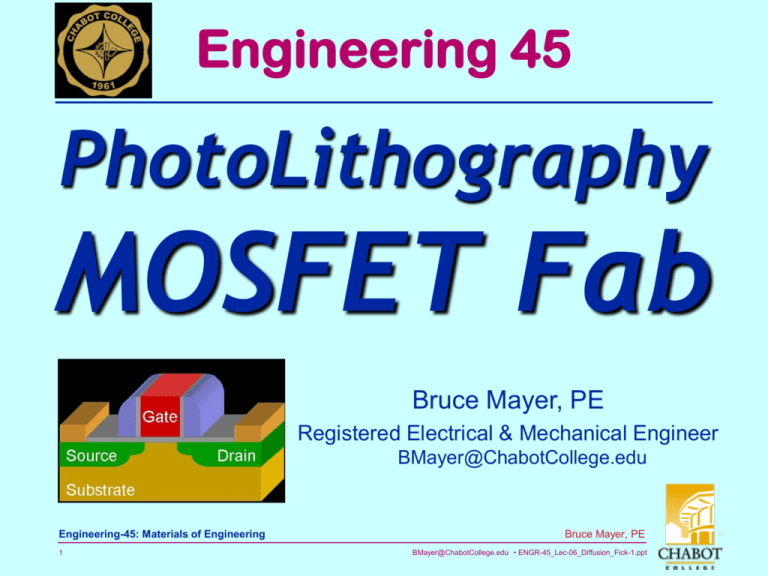
Engineering 45 PhotoLithography MOSFET Fab Bruce Mayer, PE Registered Electrical & Mechanical Engineer BMayer@ChabotCollege.edu Engineering-45: Materials of Engineering 1 Bruce Mayer, PE BMayer@ChabotCollege.edu • ENGR-45_Lec-06_Diffusion_Fick-1.ppt PhotoLithoGraphic Patterning - 1 Begin with a precise flat surface such as silicon wafer silicon substrate Engineering-45: Materials of Engineering 2 Bruce Mayer, PE BMayer@ChabotCollege.edu • ENGR-45_Lec-06_Diffusion_Fick-1.ppt PhotoLithoGraphic Patterning - 2 A THIN layer of a different material is deposited or grown on the substrate field oxide oxide silicon substrate Engineering-45: Materials of Engineering 3 Bruce Mayer, PE BMayer@ChabotCollege.edu • ENGR-45_Lec-06_Diffusion_Fick-1.ppt PhotoLithoGraphic Patterning - 3 A Thin layer of PHOTOsensitive, and acid/etch chemical RESISTING material (a.k.a. PhotoResist) is applied to the wafer photoresist oxide silicon substrate Engineering-45: Materials of Engineering 4 Bruce Mayer, PE BMayer@ChabotCollege.edu • ENGR-45_Lec-06_Diffusion_Fick-1.ppt Litho-4: Ultraviolet light Exposes photoresist through windows in a photomask Ultraviolet Light Chrome plated glass mask Shadow on photoresist Exposed area of photoresist photoresist oxide Engineering-45: Materials of Engineering silicon substrate 5 Bruce Mayer, PE BMayer@ChabotCollege.edu • ENGR-45_Lec-06_Diffusion_Fick-1.ppt PhotoLithoGraphic Patterning – 5 Exposed photoresist becomes soluble and can be easily removed by a “developer” chemical. Exposed area of photoresist Unexposed area of photoresist photoresist oxide silicon substrate Engineering-45: Materials of Engineering 6 Bruce Mayer, PE BMayer@ChabotCollege.edu • ENGR-45_Lec-06_Diffusion_Fick-1.ppt PhotoLithoGraphic Patterning – 6 Unexposed photoresist remains on surface of oxide to serve as a temporary protective mask for areas of the oxide that are not to be etched/disolved photoresist photoresist oxide silicon substrate Engineering-45: Materials of Engineering 7 Bruce Mayer, PE BMayer@ChabotCollege.edu • ENGR-45_Lec-06_Diffusion_Fick-1.ppt PhotoLithoGraphic Patterning – 7 Areas of oxide protected by photoresist remain on the silicon substrate while exposed oxide is removed by the etching process. photoresist oxide oxide siliconsubstrate substrate silicon Engineering-45: Materials of Engineering 8 Bruce Mayer, PE BMayer@ChabotCollege.edu • ENGR-45_Lec-06_Diffusion_Fick-1.ppt PhotoLithoGraphic Patterning – 8 The photoresist is removed using a “stripping process” -revealing the patterned “window” on the thin oxide layer. Oxide Layer oxide oxide siliconsubstrate substrate silicon Engineering-45: Materials of Engineering 9 Bruce Mayer, PE BMayer@ChabotCollege.edu • ENGR-45_Lec-06_Diffusion_Fick-1.ppt Intel squeezes 2 BILLION transistors onto new Itanium chip – Feb08 The new 65-nanometer Tukwila Itanium processor, which is expected to be released at the end of 2009, will run at up to 2 GHz, have dual-integrated memory controllers and use Intel's QuickPath interconnect instead of a front-side bus. The processor also will have 2 billion transistors on one chip BUT...What is a TRANSISTOR? • What KIND of Transistors are used? • HOW are the Transistors MADE? Engineering-45: Materials of Engineering 10 Bruce Mayer, PE BMayer@ChabotCollege.edu • ENGR-45_Lec-06_Diffusion_Fick-1.ppt Acknowledgement These Following Images Were Graciously Provided by • Michael W. Davidson National High Magnetic Field Laboratory 1800 E. Paul Dirac Dr. The Florida State University Tallahassee, Florida 32310 Tel: 850-644-0542 Fax: 850-644-8920 email: davidson@magnet.fsu.edu web: http://microscopy.fsu.edu Engineering-45: Materials of Engineering 11 Bruce Mayer, PE BMayer@ChabotCollege.edu • ENGR-45_Lec-06_Diffusion_Fick-1.ppt n-MOSFET Electronic Device negative channel, Metal-Oxide-Silicon, Field-Effect Transfer-resistor (Transistor) d g Vg s Vs Gate Source Electrical Current Vd Engineering-45: Materials of Engineering 12 Drain Bruce Mayer, PE BMayer@ChabotCollege.edu • ENGR-45_Lec-06_Diffusion_Fick-1.ppt 1. Form Gate & Isolation Dielectric Oxidize P-Type Silicon in Tube Furnace • 1000-1100 °C in O2 or Wafer-Vapor • Forms Insulating Layer of Silicon Dioxide (SiO2) – Yellow Layer Below Engineering-45: Materials of Engineering 13 Bruce Mayer, PE BMayer@ChabotCollege.edu • ENGR-45_Lec-06_Diffusion_Fick-1.ppt 2. Apply Photo Resist Spin on “Thick” Liquid Photo Resist (blue) and “SoftBake” to make resist plastic-like Engineering-45: Materials of Engineering 14 Bruce Mayer, PE BMayer@ChabotCollege.edu • ENGR-45_Lec-06_Diffusion_Fick-1.ppt 3. Expose the Negative PhotoResist First Mask Placed Over PhotoResist UltraViolet Light Projected onto the Mask Exposed PhotoResist Hardens (negative resist) Engineering-45: Materials of Engineering 15 Bruce Mayer, PE BMayer@ChabotCollege.edu • ENGR-45_Lec-06_Diffusion_Fick-1.ppt 4. Develop Exposed PhotoResist Unexposed (and soft) PhotoResist (PR) is Washed away by the “Developer” Solution • Leaves the exposed PR and SiO2 in tact Engineering-45: Materials of Engineering 16 Bruce Mayer, PE BMayer@ChabotCollege.edu • ENGR-45_Lec-06_Diffusion_Fick-1.ppt 5. Etch SiO2 to form Gate Dielectric Etch the Thin the SiO2 Using “Plasma Etching” Leave only a Very Thin Insulating Layer Engineering-45: Materials of Engineering 17 Bruce Mayer, PE BMayer@ChabotCollege.edu • ENGR-45_Lec-06_Diffusion_Fick-1.ppt 6. Remove Used PhotoResist Hardened PhotoResist is removed by one of: • Liquid Solvent • Gaseous Ozone “Ashing” Engineering-45: Materials of Engineering 18 Bruce Mayer, PE BMayer@ChabotCollege.edu • ENGR-45_Lec-06_Diffusion_Fick-1.ppt 7. Deposit Gate Electrode Film Deposit a Layer of Polycrystalline Silicon (red) by Low Pressure Chemical Vapor Deposition (LPCVD) Engineering-45: Materials of Engineering 19 Bruce Mayer, PE BMayer@ChabotCollege.edu • ENGR-45_Lec-06_Diffusion_Fick-1.ppt 8. Apply 2nd Layer of PhotoResist Cover PolySi with PhotoResist in Preparation for the Next Mask Step Engineering-45: Materials of Engineering 20 Bruce Mayer, PE BMayer@ChabotCollege.edu • ENGR-45_Lec-06_Diffusion_Fick-1.ppt 9. Expose PhotoResist Using Mask-2 The 2nd Mask is placed Over the PR PR exposed to UV Light Engineering-45: Materials of Engineering 21 Bruce Mayer, PE BMayer@ChabotCollege.edu • ENGR-45_Lec-06_Diffusion_Fick-1.ppt 10. Develop Gate Electrode PR Use the Developer to Wash Away UnWanted PR • Leave Behind a “T” shaped PR pattern Engineering-45: Materials of Engineering 22 Bruce Mayer, PE BMayer@ChabotCollege.edu • ENGR-45_Lec-06_Diffusion_Fick-1.ppt 11. Pattern Gate PolySilicon Use “Dry” Plasma Etching Techniques to Remove BOTH PolySi and SiO2 in areas Not Protected by PR Engineering-45: Materials of Engineering 23 Bruce Mayer, PE BMayer@ChabotCollege.edu • ENGR-45_Lec-06_Diffusion_Fick-1.ppt 12. Remove PR to Complete Gate Electrode Remove PR by Ozone Ashing Leaves a Strip of PolySi which Rises Above the Exposed Silicon Engineering-45: Materials of Engineering 24 Bruce Mayer, PE BMayer@ChabotCollege.edu • ENGR-45_Lec-06_Diffusion_Fick-1.ppt 13. Change Exposed Si from P-type to N-type Ion-Implant Phosphorus or Arsenic to Convert the Exposed Silicon to N-Type Engineering-45: Materials of Engineering 25 Bruce Mayer, PE BMayer@ChabotCollege.edu • ENGR-45_Lec-06_Diffusion_Fick-1.ppt 14. Deposit Electrical Contact Insulation Deposit SiO2 by TEOS+O3 APCVD • The SiO2 may P or P+B doped Engineering-45: Materials of Engineering 26 Bruce Mayer, PE BMayer@ChabotCollege.edu • ENGR-45_Lec-06_Diffusion_Fick-1.ppt 15. Apply Contact Via PR Apply a 3rd Layer of PhotoResist that Will be used to Form the Vertical Shafts used for Electrical Contacts Engineering-45: Materials of Engineering 27 Bruce Mayer, PE BMayer@ChabotCollege.edu • ENGR-45_Lec-06_Diffusion_Fick-1.ppt 16. Expose PR using 3rd Mask Again Exposed Masked PR to UV Light The Black Rectangles Will Define the Contact Holes Engineering-45: Materials of Engineering 28 Bruce Mayer, PE BMayer@ChabotCollege.edu • ENGR-45_Lec-06_Diffusion_Fick-1.ppt 17. Develop Contact-Via PR Develop the PR to Expose the SiO2 in the desired Contract areas Engineering-45: Materials of Engineering 29 Bruce Mayer, PE BMayer@ChabotCollege.edu • ENGR-45_Lec-06_Diffusion_Fick-1.ppt 18. Expose Silicon Thru Etching Etch the SiO2 Not Protected by the PR to Expose the underlying Silicon • PolySi at rear • N-Type Si at Front-Left & Front-Right Engineering-45: Materials of Engineering 30 Bruce Mayer, PE BMayer@ChabotCollege.edu • ENGR-45_Lec-06_Diffusion_Fick-1.ppt 19. Remove Contact-Via PR Remove the PR to Reveal Contact holes, or vias, in the insulating APCVD-SiO2 Engineering-45: Materials of Engineering 31 Bruce Mayer, PE BMayer@ChabotCollege.edu • ENGR-45_Lec-06_Diffusion_Fick-1.ppt 20. Deposit Aluminum Contact Wiring Blanket Deposit Al-Cu Alloy by Sputtering Al Contacts the Si and PolySi thru the holes in the APCVD-SiO2 Engineering-45: Materials of Engineering 32 Bruce Mayer, PE BMayer@ChabotCollege.edu • ENGR-45_Lec-06_Diffusion_Fick-1.ppt 21. Apply “Wiring” PhotoResist Apply a 4th Layer of PhotoResist that Will be used to Form the Al-Cu “wires” that Carry Electrical Current and Potential (Voltage) to the Transistor Engineering-45: Materials of Engineering 33 Bruce Mayer, PE BMayer@ChabotCollege.edu • ENGR-45_Lec-06_Diffusion_Fick-1.ppt 22. Metallization Exposure Expose the PR using the Metallization Mask Engineering-45: Materials of Engineering 34 Bruce Mayer, PE BMayer@ChabotCollege.edu • ENGR-45_Lec-06_Diffusion_Fick-1.ppt 23. Develop Metallization PR Develop PR Exposing Regions of the Al-Cu Metal for Subsequent Removal Engineering-45: Materials of Engineering 35 Bruce Mayer, PE BMayer@ChabotCollege.edu • ENGR-45_Lec-06_Diffusion_Fick-1.ppt 24. Etch UnProtected Al-Cu to Form “Wires” The Final Etching Step Removes the Unwanted Metal; Leaving only Metal used for • Contacting thru the Vertical-Shaft Vias the Silicon Source/Drain and Poly-Si Gate • Forming Strips of Al-Cu that act as Wires Engineering-45: Materials of Engineering 36 Bruce Mayer, PE BMayer@ChabotCollege.edu • ENGR-45_Lec-06_Diffusion_Fick-1.ppt 25. Remove Remaining Resist Xsistor Done Remove the Remaining Metallization Resist, Completing the n-MOSFET Transistor • Millions of transistors can be formed Simultaneously Engineering-45: Materials of Engineering 37 Bruce Mayer, PE BMayer@ChabotCollege.edu • ENGR-45_Lec-06_Diffusion_Fick-1.ppt

