MPI Sessional-1 September 2015
advertisement
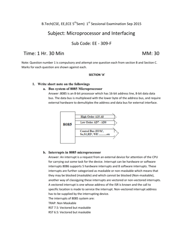
B.Tech(CSE, EE,ECE 5thSem) 1st Sessional Examination Sep 2015 Subject: Microprocessor and Interfacing Sub Code: EE - 309-F Time: 1 Hr. 30 Min MM: 30 Note: Question number 1 is compulsory and attempt one question each from section B and Section C. Marks for each question are shown against each. SECTION ‘A’ 1. Write short note on the followings a. Bus system of 8085 Microprocessor Answer :8085 is an 8-bit processor which has 16-bit address line, 8-bit data data bus. The data bus is multiplexed with the lower byte of the address bus, and require external hardware to demultiplex the address and data bus for external interface. b. Interrupts in 8085 microprocessor Answer: An interrupt is a request from an external device for attention of the CPU for carrying out some task for the device. Interrupt can be hardware or software interrupts 8086 supports 5 hardware interrupts and 8 software interrupts. These interrupts are further categorized as maskable or non-maskable which means that they may be blocked (maskable) and which cannot be blocked (Non-maskable), another way of classigying these interrupts are vectored or non-vectored interrupts. A vectored interrupt is one whose address of the ISR is known and the call to specific location is made to service the interrupt. Non-vectored interrupt address has to be supplied by the interrupting device. The interrupts of 8085 system are: TRAP: Non Maskable RST 7.5: Vectored but maskable RST 6.5: Vectored but maskable RST 5.5: Vectored but maskable INTR: c. Flag register of 8086 Microprocessor Answer: Flag register indicate the status of the current operation performed by the CPU(to be more specific inside the ALU). 8086 has a 16-bit flag register of which only 9-bits are used as Flag. 5 of the flags are same as in 8085 microprocessor and four new flags are added. The flag register of 8086 microprocessor is shown below: 15 - 14 - 13 - 12 OF 11 DF 10 IF 9 TF 8 S 7 Z 6 - 5 AC 4 - 3 P 2 - 1 Cy These flags are control Flags: i. DF: data direction flag used to point to the beginning or end of array ii. IF: Interrupt Flag, by setting or clearing this flag the interrupt can be disabled or enabled. iii. TF: Trap Flag is used for single step for debugging operations. Data Flags: i. Carry i. Parity ii. Auxiliary Flag iii. Zero Flag iv. Sign Flag v. Overflow Flag d. Calculation of Physical address in 8086 Microprocessor . 2 Answer: The physical address in 8086 system is calculated using the following formula Physical Address = Segment Register Value x 10 + Offset For example, if Value in Segment register=1234h, offset is 2345h, then : Segment address x 10 = 1234h x 10h = 12340 offset = + 2345 Physical Address = 14385h This is a 20-bit address. SECTION ‘B’ 2. (a) Explain the function of ALE and IO/M’ signals of the 8085 microprocessor. Also explain the need to demultiplex the AD7-AD0 lines. 5 Answer : A high ALE signal is generated during the first T state of a machine cycle by the CPU to enable the latch. During this cycle this signal will activate the latch so that the low order address bus can be separated from the data bus. IO/M’ signal is a control signal which along with S1,S0, RD’ and WR’ is used for selecting memory or I/O device for read write operation. Need for Multiplexing: The low order address and the data bus are internally multiplexed in 8086 microprocessor. This multiplexing is done to reduce the number of pins on the IC package. However to interface with the external environment, these buses are required to be separated for proper timing synchronization and operation. This separation of the low order address bus and data bus is called de-multiplexing the buses. To de-multiplexing the address and data bus the CPU generates a high ALE signal to enable the latch to latch the address during the first T state of the machine cycle. This de-multiplexing is shown in the following figure. (b) (c) WAP to add 10 numbers stored in memory, and store the sum at address 2050h and carry if any at address 2051h. 5 Answer: Assuming that the 10 numbers are stored in memory starting at address 2020h. As we add the carry if any will be incremented in register ‘B’ and accumulator will contain the sum of the numbers. Finally the Sum will be stored at 2050h and carries will be stored at 2051h. The following chart shows the logic for the operation. The complete program is given beside the flowchart. 3. (a) Write an assembly language program to count the number of 1’s and zeros in a given data. 5 (b) What do you understand by the word addressing mode? Explain the different addressing mode of 8085 microprocessor. 5 Answer: Addressing Modes: As we are aware that a data item may reside in internal registers, RAM, may come from input device or can be assigned as immediate as part of an instruction. For accessing each type there is a well defined way or method. Therefore, we can define addressing modes as the methods of accessing the data byte(operands). Addressing mode are of the following type in 8085 microprocessor. 1. Immediate addressing mode In this addressing mode the data byte is defined as part of the instruction. 8085 microprocessor supports an immediate to register or immediate to memory assignment, and use the instruction MVI for this purpose. The general Syntax is : MVI Reg/Mem 8-bit Data Example: MVI A, 55h ; Transfers an immediate number 55h to Accumulator MVI B, 55h ; Transfers an immediate number 55h to Register B MVI M, 55h ; Transfers an immediate number 55h to Memory pointed by HL pair 2. Implicit addressing mode: This addressing mode does not specify any additional data, but the data is implied with the instruction, the data is referred by the name of the instruction. As an example CLA stands for clear the accumulator. Here no additional reference is made to locate the data. Instruction of this type are 1-byte instructions. Examples: CMA,STC, CLC, RLC, RRC,RAL, RAR 3. Register addressing mode: This addressing mode is used t transfer the data item from source register to a destination register. The source register must be loaded with data before using this instruction. This addressing mode uses MOV instruction for transferring data among registers. Syntax: MOV Rd, Rs Here Rs is source register from the general purpose registers and Rd is the destination register from the general purpose registers. Examples: MOV A, B ; Transfers 8-bit data from register B to accumulator MOV D, E ; Transfers 8-bit data from register E to register D 4. Direct addressing Mode The direct addressing mode refers to the data from / to the memory for transfer to or from the registers. Use of this addressing mode require setting the memory pointer. 8085 uses MOV instruction for this purpose. Syntax: MOV Rd, M; where Rd is the destination register and M is the memory location pointed by HL MOV M, Rs; where M is the memory location pointed by HL, and Rs is the source register. Usage example: LXI H, 2050 ; Set the memory pointer MOV B, M ; Transers data from memory location 2050h into register B. This instruction also expects the data byte at location 2050. 5. Indirect memory addressing mode In this addressing mode the data is accessed indirectly from the memory. The address from where the data is to be fetched is to be found at other place. 8085 uses instructions such as LDAX, STAX, LHLD, SHLD for indirect addressing. These are explained below: Example LDAX [Rp] ; Will load accumulator with data from address given in register pair Rp(BC, DE, HL) STAX [Rp] ; Will store data given in accumulator in memory at address given in register pair Rp. LHLD [Rp] ; Loads Register L from address given in Rp, then increment Rp and load H from there. LHLD [Rp] ; Stores Register L from at address given in Rp, then increment Rp and stores H there. SECTION ‘C’ 4. (a) Explain the internal architecture of 8086 Microprocessor 5 Answer: The system architecture defines how the processor and components relates to each other. The different components of 8086 are grouped and partitioned logically into two processing units. They are the Bus Interface Unit (BIU) and the Execution Unit (EU) as shown in figure below: Execution Unit (EU): The EU consists of a set of general purpose registers (AX, BX, CX and DX) the base and index pointers, the ALU, control unit and the flag register. The EU is where actual processing take place. The instructions from the instruction queue and the data that have been fetched by the BIU are accepted by EU and operate on the data as per the instructions. After an operation the processed data (result) can be taken to memory or other peripheral device for later use. As stated above it has 4 components: Control circuitry, ALU, Flag registers and general purpose registers. The basic functions of these different components are: : 1. Control Circuits: it directs all the internal operations. 2. ALU: It is where all logic and arithmetic operations are performed. 3. General purpose registers: They are used to store data during execution. 4. Flag registers: It has a 16bit flag register containing 9 flags that are set for certain conditions during any operation. Bus interface unit (BIU): The basic purpose of this unit is to generate the address of the instructions and the data. It provides a full 16 bit bidirectional data bus and 20 bit address bus (i.e. Address/Data bus is demultiplexed here). The BIU is responsible for the fetching of the data and instructions from the memory. It contains the following components. 1. Segment registers: There are four segment register namely code segment register(CS), data segment register, extra segment register, stack segment register.These register contain the 16 bit segment begining address. The full 20 bit address is however obtained by multiplying segment register value by (10)hex and adding the offset/(instruction pointer value) 2. Multiplier/adder circuit: The BIU contain a multiplier/ adder unit for calculation of the instruction/data address. 3. Instruction Pointer: The instruction pointer points to the address of the instruction. It is a 16 bit address and thus can point to the 64KB address within a segment. 4. Queue : 8086 has a 6 byte queue, use of the queue allows prefetching of instruction from the memory while the execution of previous instruction is going on in the execution unit. (b) Explain the Programming Model of 8085 Microprocessor 5 The programming model of 8085 consist of an 8-bit accumulator, one flag register, 6 general 8-bit purpose registers, and two 16-bit special purpose registers. These registers are critically required when programming a 8085 processor. The different register in the programming model are explained below: Accumulator: Accumulator is an 8-bit register. For processing the numbers, 8085 assumes that one of the numbers is in accumulator. After processing, the result is accumulated in accumulator. General purpose registers: 8085 has six general purpose registers these are Register B,C,D,E,H,L.All these registers are 8-bits each. These registers can also be used in pair as BC, DE and HL for use as 16bit data operations. Program Counter (PC) This 16-bit register deals with sequencing the execution of instructions. This register is a memory pointer. Memory locations have 16-bit addresses, and that is why this is a 16-bit register. The microprocessor uses this register to sequence the execution of the instructions. The function of the program counter is to point to the memory address from which the next byte is to be fetched. When a byte (machine code) is being fetched, the program counter is incremented by one to point to the next memory location Stack Pointer (SP) The stack pointer is also a 16-bit register used as a memory pointer. It points to a memory location in R/W memory, called the stack. The beginning of the stack is defined by loading 16-bit address in the stack pointer. The 8085 uses PUSH and POP instructions for stack operations. Flag Register: ALU of 8085 contains a special register called a “Flag register” and is an 8-bit register. At the time of design of 8085 only five flags of this register were used and the rest three were reserved. These flags are set or reset after an operation according to data conditions of the result in the accumulator and other registers. They are called Zero(Z), Carry (CY), Sign (S), Parity (P), and Auxiliary Carry (AC) flags; their bit positions in the flag register are shown in the Figure below. The most commonly used flags are Zero, Carry, and Sign. The microprocessor uses these flags to test data conditions 5. Explain the flag register of 8086 microprocessor. Register B has 65H and the accumulator has 97H. Subtract the content of register B from the content of the accumulator. Also give the flag status in 8086 Microprocessor system 10 Answer: Register B = +65 Register C = +97 C-B using 2’s complement = = 01000001 01100001 -65 10111110 + 1 = 10111111 Adding +97 = 01100001 - 65 = 10111111 97-65 = 1 00100000 Neglecting the carry, we get the answer as 00100000, here MSB is ‘0’ indicating result is +ve, and the magnitude of the result is 32 The status as indicated by the flag register is : 15 14 13 12 11 10 9 8 7 6 5 4 3 2 1 0 OF DF IF TF S Z AC P Cr 0 0 0 0 0 0 1 0 1
