Bipolar transistor - Analog Innovations
advertisement
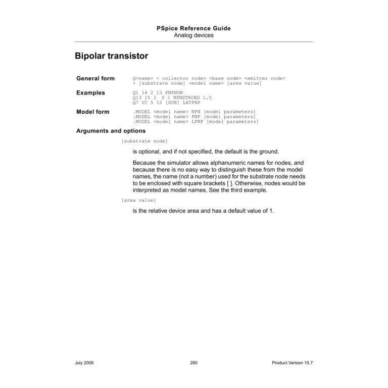
PSpice Reference Guide Analog devices Bipolar transistor General form Q<name> < collector node> <base node> <emitter node> + [substrate node] <model name> [area value] Examples Q1 14 2 13 PNPNOM Q13 15 3 0 1 NPNSTRONG 1.5 Q7 VC 5 12 [SUB] LATPNP Model form .MODEL <model name> NPN [model parameters] .MODEL <model name> PNP [model parameters] .MODEL <model name> LPNP [model parameters] Arguments and options [substrate node] is optional, and if not specified, the default is the ground. Because the simulator allows alphanumeric names for nodes, and because there is no easy way to distinguish these from the model names, the name (not a number) used for the substrate node needs to be enclosed with square brackets [ ]. Otherwise, nodes would be interpreted as model names. See the third example. [area value] is the relative device area and has a default value of 1. July 2006 260 Product Version 15.7 PSpice Reference Guide Analog devices Comments The simulator supports the following two models for a bipolar transistor: Level 1: Gummel-Poon model Level 2: Mextram model Mextram is an extended model that can describe various features of the modern down-scaled transistor, such as avalanche, collector epilayer current, and overlap capacitances. The Mextram model supported by this simulator is level 504. For more information about Mextram 504, you can visit http://www.semiconductors.philips.com/Philips_Models/ bipolar/mextram/. Note: Simulations might take more time for circuit involving the Mextram model in comparison to Gummel-Poon due to the complex nature of the equations. The convergence issues might also be more. Following is a list of effects that are better modelled by Mextram: July 2006 ■ Temperature ■ Charge storage ■ Substrate ■ Parasitic PNP ■ Low-level, non-ideal base currents ■ Hard- and quasi-saturation ■ Weak avalanche ■ Hot carrier effects in the collector epilayer ■ Explicit modelling of inactive regions ■ Split base-collector depletion capacitance ■ Current crowding and conductivity modulation for base resistance ■ Distributed high frequency effects in the intrinsic base (high frequency current crowding and excess phase shift) ■ High-injection ■ Built-in electric field in base region ■ Bias-dependent Early effect 261 Product Version 15.7 PSpice Reference Guide Analog devices Description Note: The self heating effect of Mextram model level 504 is not supported in release 10.5. As a result, the self heating effect equations and parameters are not implemented in this simulation The bipolar transistor is modeled as an intrinsic transistor using ohmic resistances in series with the collector (RC/area), with the base (value varies with current, see Bipolar transistor equations on page 276), and with the emitter (RE/area). Model Level 1 Collector Qw Iepi (if RCO > 0) Qo Cjs Ibc1/BR Cjc Base Ibc2 Rb Cje Ibe2 (IbeIbc1)/Kqb Ibe1/BF Substrate (NPN and PNP only) RE Substrate Emitter (LPNP only) Note: Positive current is current flowing into a terminal. Model Level 2 The equivalent circuit for model level 2 shows the intrinsic part of the transistor and the base, emitter, and the collector or epilayer resistance. July 2006 262 Product Version 15.7 PSpice Reference Guide Analog devices C CBCO B E CBEO n+ emitter p base QtgS RE E1 ISB1 RBC B1 QE IB1B2 QBE QBC RCC XQTEX QEX C1 S ISF QTS IB1 IN QTE IAVL QTC IEX+ IB3 QTEX Isub IB2 QEPI C2 IC1C2 n epilayer n+ buried layer p substrate You can use two flags, EXMOD and EXPHI, to introduce additional elements to the schematic of a transistor in model level 2. July 2006 263 Product Version 15.7 PSpice Reference Guide Analog devices C CBCO B E CBEO p base n+ emitter S Q tE RE E1 S QE I B1 RBc QB1B2 B1 QBE RCc XIex Qtex QtE IN B2 Isub Iex+IB3 XIsub ISf Iavl Qepi Qex C2 n epilayer IC1C2 n+ buried layer C1 S IB1 QBC QtC XQtex XQex IB2 QtS p substrate The small signal equivalent circuit is shown by the following figure. S B rB CBC B2 CBE β -----gm g m v B2E1 g µ v C1E1 Cts RCc 1 --------g out E1 RE E July 2006 264 Product Version 15.7 PSpice Reference Guide Analog devices The small signal model uses the following small-signal parameters: Note: The conductances are derivatives with respect to three different biases, namely, base-emitter denoted by the subscript x, internal base-collector denoted by the subscript y, and base-collector denoted by the subscript z. The transconductance, g m , is given by the following equation: g Rcv,y ( g x – g µ, x + g z – g µ, z ) – ( g Rcv,x + g Rcv,z ) ( g y – g µ, y ) g m = ---------------------------------------------------------------------------------------------------------------------------------------------g Rcv,y + g µ, y – g y The base conductance, g π , is given by the following equation: dy dy g π = gS π + g π, x + g µ, x + g π, z + g µ, z + ( g π, y + g µ, y ) ------ + -----dx dz The current amplification, β , is given by the following equation: β = gm ⁄ gπ The output conductance, g out, is given by the following equation: g out ( g y – g µ, y )g Rcv,z – ( g z – g µ, z )g Rcv,y = ---------------------------------------------------------------------------------------g Rcv,y + g µ, y – g y The feedback transconductance, g µ , is given by the following equation: dy g µ = g π, z + g µ, z + ( g π, y + g µ, y ) ⋅ ------ + g µex + X g µex dz The base-emitter capacitance, CBE, is given by the following equation: dy S C BE = C BE,x + C BE + C BC,x + ( C BE,y + C BC,y ) ⋅ ------ + C BEO dx July 2006 265 Product Version 15.7 PSpice Reference Guide Analog devices The base-collector capacitance, CBC, is given by the following equation: dy C BC = ( C BE,y + C BC,y ) ⋅ ------ + C BC,z + C BCex + X C BCex + C BCO dz In addition to the listed parameters, the cut-off frequency fT is another important design parameter. The cut-off frequency is a compound smallsignal quantity and can be represented in terms of the total transit time, as given by the following equation: f T = 1 ⁄ ( 2πτ T ) The total transit time, τ T , is given by the following equation: S τ T = C BE ⋅ ( r x + r b1b2 ) + ( C BE,x + C BC,x ) ⋅ r x ( C BE,y + C BC,y ) ⋅ r y + ( C BE,z + C BC,z ) ⋅ r z + C BCex r ex X C BCex X r ex + ( C BEO + C BCO ) ( X r ex – R Cc ) For model parameters with alternate names, such as VAF and VA (the alternate name is shown by using parentheses), either name can be used. For model types NPN and PNP, the isolation junction capacitance is connected between the intrinsic-collector and substrate nodes. This is the same as in SPICE2, or SPICE3, and works well for vertical IC transistor structures. For lateral IC transistor structures there is a third model, LPNP, where the isolation junction capacitance is connected between the intrinsic-base and substrate nodes. July 2006 266 Product Version 15.7 PSpice Reference Guide Analog devices Capture parts The following table lists the set of bipolar transistor breakout parts designed for customizing model parameters for simulation. These are useful for setting up Monte Carlo and worst-case analyses with device and/or lot tolerances specified for individual model parameters. Part name Model type Property Property description QBREAKL LPNP AREA MODEL area scaling factor LNP model name QBREAKN QBREAKN3 QBREAKN4 NPN AREA MODEL area scaling factor NPN model name QBREAKP QBREAKP3 QBREAKP4 PNP AREA MODEL area scaling factor PNP model name Setting operating temperature Operating temperature can be set to be different from the global circuit temperature by defining one of the model parameters: T_ABS, T_REL_GLOBAL, or T_REL_LOCAL. Additionally, model parameters can be assigned unique measurement temperatures using the T_MEASURED model parameter. See Bipolar transistor model parameters on page 268 for more information. July 2006 267 Product Version 15.7 PSpice Reference Guide Analog devices Bipolar transistor model parameters Model level 1 Model parameters1 Description Units Default AF flicker noise exponent 1.0 BF ideal maximum forward beta 100.0 BR ideal maximum reverse beta 1.0 CJC base-collector zero-bias p-n capacitance farad 0.0 CJE base-emitter zero-bias p-n capacitance farad 0.0 CJS (CCS) substrate zero-bias p-n capacitance farad 0.0 CN quasi-saturation temperature coefficient for hole mobility 2.42 NPN 2.20 PNP D quasi-saturation temperature coefficient for scattering-limited hole carrier velocity 0.87 NPN 0.52 PNP EG bandgap voltage (barrier height) FC forward-bias depletion capacitor coefficient 0.5 GAMMA epitaxial region doping factor 1E-11 IKF (IK) corner for forward-beta high-current roll-off amp infinite IKR corner for reverse-beta high-current roll-off amp infinite IRB current at which Rb falls halfway to amp infinite IS transport saturation current amp 1E-16 ISC (C4) † base-collector leakage saturation current amp 0.0 ISE (C2) † base-emitter leakage saturation current amp 0.0 ISS substrate p-n saturation current amp 0.0 ITF transit time dependency on Ic amp 0.0 KF flicker noise coefficient July 2006 268 eV 1.11 0.0 Product Version 15.7 PSpice Reference Guide Analog devices Model parameters1 Description Units Default MJC (MC) base-collector p-n grading factor 0.33 MJE (ME) base-emitter p-n grading factor 0.33 MJS (MS) substrate p-n grading factor 0.0 NC base-collector leakage emission coefficient 2.0 NE base-emitter leakage emission coefficient 1.5 NF forward current emission coefficient 1.0 NK high-current roll-off coefficient 0.5 NR reverse current emission coefficient 1.0 NS substrate p-n emission coefficient 1.0 PTF excess phase @ 1/(2π·TF)Hz degree 0.0 QCO epitaxial region charge factor coulom b 0.0 QUASIMOD quasi-saturation model flag for temperature dependence 0 if QUASIMOD = 0, then no GAMMA, RCO, VO temperature dependence if QUASIMOD = 1, then include GAMMA, RCO, VO temperature dependence RB zero-bias (maximum) base resistance ohm 0.0 RBM minimum base resistance ohm RB RC collector ohmic resistance ohm 0.0 RCO ‡ epitaxial region resistance ohm 0.0 RE emitter ohmic resistance ohm 0.0 TF ideal forward transit time sec 0.0 TR ideal reverse transit time sec 0.0 TRB1 RB temperature coefficient (linear) ˚C-1 0.0 TRB2 RB temperature coefficient (quadratic) ˚C-2 0.0 TRC1 RC temperature coefficient (linear) ˚C-1 0.0 TRC2 RC temperature coefficient (quadratic) ˚C-2 0.0 July 2006 269 Product Version 15.7 PSpice Reference Guide Analog devices Model parameters1 Description Units Default TRE1 RE temperature coefficient (linear) ˚C-1 0.0 TRE2 RE temperature coefficient (quadratic) ˚C-2 0.0 TRM1 RBM temperature coefficient (linear) ˚C-1 0.0 TRM2 RBM temperature coefficient (quadratic) ˚C-2 0.0 T_ABS absolute temperature ˚C T_MEASURED measured temperature ˚C T_REL_GLOBAL relative to current temperature ˚C T_REL_LOCAL relative to AKO model temperature ˚C VAF (VA) forward Early voltage volt infinite VAR (VB) reverse Early voltage volt infinite VG quasi-saturation extrapolated bandgap voltage at V 0˚ K 1.206 VJC (PC) base-collector built-in potential volt 0.75 VJE (PE) base-emitter built-in potential volt 0.75 VJS (PS) substrate p-n built-in potential volt 0.75 VO carrier mobility knee voltage volt 10.0 VTF transit time dependency on Vbc volt infinite XCJC fraction of CJC connected internally to Rb 1.0 XCJC2 fraction of CJC connected internally to Rb 1.0 XCJS fraction of CJS connected internally to Rc XTB forward and reverse beta temperature coefficient 0.0 XTF transit time bias dependence coefficient 0.0 XTI (PT) IS temperature effect exponent 3.0 1. For information on T_MEASURED, T_ABS, T_REL_GLOBAL, and T_REL_LOCAL, see .MODEL (model definition) on page 55. † The parameters ISE (C2) and ISC (C4) can be set to be greater than one. In this case, they are interpreted as multipliers of IS instead of absolute currents: that is, if ISE is greater than one, then it is replaced by ISE·IS. Likewise for ISC. ‡ If the model parameter RCO is specified, then quasi-saturation effects are included. July 2006 270 Product Version 15.7 PSpice Reference Guide Analog devices Distribution of the CJC capacitance The distribution of the CJC capacitance is specified by XCJC and XCJC2. The model parameter XCJC2 is used like XCJC. The differences between the two parameters are as follows. Branch XCJC XCJC2 intrinsic base to intrinsic collector XCJC*CJC XCJC2*CJC extrinsic base to intrinsic collector (1.0 – XCJC)*CJC not applicable extrinsic base to extrinsic collector not applicable (1.0 – XCJC2)*CJC When XCJC2 is specified in the range 0 < XCJC2 < 1.0, XCJC is ignored. Also, the extrinsic base to extrinsic collector capacitance (Cbx2) and the gain-bandwidth product (Ft2) are included in the operating point information (in the output listing generated during a Bias Point Detail analysis, .OP (bias point) on page 66). For backward compatibility, the parameter XCJC and the associated calculation of Cbx and Ft remain unchanged. Cbx and Ft appears in the output listing only when XCJC is specified. The use of XCJC2 produces more accurate results because Cbx2 (the fraction of CJC associated with the intrinsic collector node) now equals the ratio of the device’s emitter area-to-base area. This results in a better correlation between the measured data and the gain bandwidth product (Ft2) calculated by PSpice. which is valid in the range 0 ≤ XCJS ≤ 1.0, specifies a portion of the CJS capacitance to be between the external substrate and external collector nodes instead of between the external substrate and internal collector nodes. When XJCS is 1, CJS is applied totally between the external substrate and internal collector nodes. When XCJS is 0, CJS is applied totally between the external substrate and external collector codes. XCJS, Model level 2 Model Parameters Description Units Default Value Level 2: general parameters EXAVL flag for the extended modelling of avalanche currents 0 EXMOD flag for the extended modelling of the external regions 0 July 2006 271 Product Version 15.7 PSpice Reference Guide Analog devices Model Parameters Description Units Default Value EXPHI flag for the extended modelling of distributed HF effects in transients 0 MULT number of parallel transistors modelled together 1.0 Level 2: intrinsic and extrinsic charge and current split parameters XCJC sidewall fraction collector-base depletion farad capacitance that is under the emitter 32E-03 XCJE sidewall fraction of the emitter-base depletion capacitance farad 0.4 XEXT fraction of external charges between B and C1 coulomb 0.63 XIBI sidewall fraction of the ideal base current amp 0.0 Level 2: current parameters BF current gain of ideal forward base current 215.0 BRI (BR) current gain of ideal reverse base current 7.0 IBF saturation current of the non-ideal forward base current 2.7E-15 IBR saturation current of the non-ideal reverse base current amp 1.0E-15 IK (IKF) intrinsic transistor high-injection knee current amp 0.1 IKS parasitic PNP transistor high-knee current amp 250.0E-6 IS intrinsic transistor saturation current amp 22.0E-18 ISS parasitic PNP transistor saturation current amp 48.0E-18 MLF non-ideality factor of the non-ideal forward base current SFH Voltage describing the curvature of the avalanche current July 2006 272 2.0 volt 0.3 Product Version 15.7 PSpice Reference Guide Analog devices Model Parameters Description Units Default Value VAVL Voltage for the curvature of the avalanche current volt 3.0 VEF (VAF) forward early voltage of the intrinsic transistor volt 44.0 VER (VAR) reverse early voltage of the intrinsic transistor volt 2.5 VLR non-ideal base current cross-over voltage volt 0.2 WAVL effective width of epilayer for avalanche current m 1.1E-6 Level 2: resistance parameters (variable and constant) AXI smoothing parameters for the epilayer model 0.3 IHC epilayer critical current for hot-carriers amp 4.0E-3 RBC external base constant resistance ohm 23.0 RBV pinched base low current resistance (under the emitter) ohm 18.0 RCC (RC) external collector constant resistance ohm 12 RCV epilayer low current resistance ohm 150.0 RE external emitter constant resistance ohm 5.0 SCRCV epilayer space charge resistance ohm 1250.0 Level 2: depletion capacitance parameters CBCO base-collector overlap capacitance farad 0.0 CBEO base-emitter overlap capacitance farad 0.0 CJC collector-base junction depletion capacitance at zero bias farad 78.0E-15 CJE emitter-base junction depletion capacitance at zero bias farad 73.0E-15 CJS collector-substrate junction depletion capacitance at zero bias farad 315.0E-15 July 2006 273 Product Version 15.7 PSpice Reference Guide Analog devices Model Parameters Description Units Default Value MC (MJC) collector depletion charge current modulation factor 0.5 PC (VJC) collector-base depletion capacitance grading coefficient 0.5 PE (VJE) emitter-base depletion capacitance grading coefficient 0.4 PS (VJS) collector-substrate depletion capacitance grading coefficient 0.34 VDC built-in diffusion voltage collector-base volt 0.68 VDE built-in diffusion voltage emitter-base volt 0.95 VDS built-in diffusion voltage emittersubstrate volt 0.62 XP (XC) constant fraction of collector-base depletion capacitance farad 0.35 Level 2: transit time parameters (diffusion charges) TAUB base transmit time sec 4.2E-12 TAUE emitter charge transmit time sec 2.0E-12 TEPI collector epilayer transmit time sec 41.0E-12 TAUR reverse transmit time sec 520.0E-12 MTAU emitter charge non-ideality factor 1.0 Level 2: noise parameters AF flickernoise exponent 2.0 KF ideal base current flickernoise coefficient 2.0E-11 KFN non-ideal base current flickernoise coefficient 2.0E-11 Level 2: temperature parameters AB temperature coefficient of RB (pinched base low current resistance) °C –1 1.0 AC temperature coefficient of RCC (external °C collector constant resistance) –1 2.0 July 2006 274 Product Version 15.7 PSpice Reference Guide Analog devices Model Parameters Description Units Default Value AE temperature coefficient of RE (external emitter constance resistance) °C –1 0.0 AEPI temperature coefficient of RCV (epilayer °C low current resistance) –1 2.5 AEX temperature coefficient of RBC (external °C base constant resistance) –1 0.62 AQBO zero bias base charge temperature coefficient °C –1 0.3 AS temperature coefficient of the mobility related to the substrate currents °C –1 1.58 DVGBF band-gap voltage difference for forward current gain volt 0.05 DVGBR band-gap voltage difference for reverse current gain volt 0.045 DVGTE band-gap voltage difference for emitter charge volt 0.05 DTA difference between device and ambient temperature °C 0.0 TREF reference temperature °C 25.0 if a value is defined for .temp, it will override the value specified in the TREF parameter VGB base band-gap voltage volt 1.17 VGC collector band-gap voltage volt 1.18 VGJ base-emitter junction recombination band-gap voltage volt 1.15 VGS substrate band-gap voltage volt 1.20 Level 2: SiGe parameters DEG base band-gap difference 0.0 XREC base recombination prefactor 0.0 July 2006 275 Product Version 15.7 PSpice Reference Guide Analog devices Bipolar transistor equations Model level 1 The equations in this section describe an NPN transistor. For the PNP and LPNP devices, reverse the signs of all voltages and currents. The following variables are used: Vbe = intrinsic base-intrinsic emitter voltage Vbc = intrinsic base-intrinsic collector voltage Vbs = intrinsic base-substrate voltage Vbw = intrinsic base-extrinsic collector voltage (quasi-saturation only) Vbx = extrinsic base-intrinsic collector voltage Vce = intrinsic collector-intrinsic emitter voltage Vjs = (NPN) intrinsic collector-substrate voltage = (PNP) intrinsic substrate-collector voltage = (LPNP) intrinsic base-substrate voltage Vt = k·T/q (thermal voltage) k = Boltzmann’s constant q = electron charge T = analysis temperature (˚K) Tnom = nominal temperature (set using the TNOM option) Other variables are listed in Bipolar transistor model parameters on page 268. Note: Positive current is current flowing into a terminal. Bipolar transistor equations for DC current Ib = base current = area·(Ibe1/BF + Ibe2 + Ibc1/BR + Ibc2) Ic = collector current = area·(Ibe1/Kqb - Ibc1/Kqb - Ibc1/BR - Ibc2) Ibe1 = forward diffusion current = IS·(eVbe/(NF·Vt)-1) Ibe2 = non-ideal base-emitter current = ISE·(eVbe/(NE·Vt)-1) July 2006 276 Product Version 15.7 PSpice Reference Guide Analog devices Bipolar transistor equations for DC current Ibc1 = reverse diffusion current = IS·(eVbc/(NR·Vt)-1) Ibc2 = non-ideal base-collector current = ISC·(eVbc/(NC·Vt)-1) Kqb = base charge factor = Kq1·(1+(1+4·Kq2)NK)/2 Kq1 = 1/(1 - Vbc/VAF - Vbe/VAR) Kq2 = Ibe1/IKF + Ibc1/IKR Is = substrate current = area·ISS·(eVjs/(NS·Vt)-1) Rb = actual base parasitic resistance Case 1 for: IRB = infinite (default value) then: Rb = (RBM + (RB-RBM)/Kqb)/area Case 2 For: IRB > 0 then: tan ( x ) – x Rb = (RBM + 3·(RB-RBM)· ------------------------------ x ⋅ ( tan ( x ) ) 2 )/area where: ( 1 + ( 144 ⁄ π 2 ) ⋅ Ib ⁄ ( area ⋅ IRB ) ) 1 / 2 – 1 ( 24 ⁄ π 2 ) ⋅ ( Ib ⁄ ( area ⋅ IRB ) ) 1 / 2 x = ------------------------------------------------------------------------------------------------ Bipolar transistor equations for capacitance All capacitances, except Cbx, are between terminals of the intrinsic transistor which is inside of the collector, base, and emitter parasitic resistances. Cbx is between the intrinsic collector and the extrinsic base. base-emitter capacitance Cbe = base-emitter capacitance = Ctbe + area·Cjbe Ctbe = transit time capacitance = tf·Gbe July 2006 277 Product Version 15.7 PSpice Reference Guide Analog devices tf = effective TF = TF·(1+XTF·(Ibe1/(Ibe1+area·ITF))2·eVbc/(1.44·VTF)) Gbe = DC base-emitter conductance = (dIbe)/(dVb) Ibe = Ibe1 + Ibe2 Cjbe = CJE·(1-Vbe/VJE)-MJE IF Vbe < FC·VJE Cjbe = CJE·(1-FC)-(1+MJE)·(1-FC·(1+MJE) +MJE·Vbe/ IF Vbe > FC·VJE VJE) base-collector capacitance Cbc = base-collector capacitance = Ctbc + area·XCJC·Cjbc Ctbc = transit time capacitance = TR·Gbc Gbc = DC base-collector conductance = (dIbc)/ (dVbc) IF Vbc < FC·VJC Cjbc = CJC·(1-Vbc/VJC)-MJC Cjbc = CJC·(1-FC)-(1+MJC)·(1 FC·(1+MJC)+MJC·Vbc/VJC) IF Vbc > FC·VJC extrinsic-base to intrinsic-collector capacitance Cbx = extrinsic-base to intrinsic-collector capacitance = area·(1-XCJC)·Cjbx IF Vbx < FC·VJC Cjbx = CJC·(1-Vbx/VJC)MJC Cjbx = CJC·(1-FC)-(1+MJC)·(1-FC·(1+MJC)+MJC·Vbx/VJC) IF Vbx > FC·VJC substrate junction capacitance Cjs = substrate junction capacitance = area·Cjjs Cjjs = CJS·(1-Vjs/VJS)-MJS(assumes FC = 0) IF Vjs < 0 Cjjs = CJS·(1+MJS·Vjs/VJS) IF Vjs > 0 Bipolar transistor equations for quasi-saturation effect Quasi-saturation is an operating region where the internal base-collector metallurgical junction is forward biased, while the external base-collector terminal remains reverse biased. This effect is modeled by extending the intrinsic Gummel-Poon model, adding a new internal node, a controlled current source, Iepi, and two controlled capacitances, represented by the July 2006 278 Product Version 15.7 PSpice Reference Guide Analog devices charges Qo and Qw. These additions are only included if the model parameter RCO is specified. See reference [3] of Model level 2 on page 280 for the derivation of this extension. Iepi = area·(VO·(Vt·(K(Vbc)-K(Vbn)-ln((1+K(Vbc))/(1+K(Vbn))))+Vbc-Vbn))/RCO·(|Vbc-Vbn|+VO) Qo = area·QCO·( K(Vbc)-1-GAMMA/2 ) Qw = area·QCO·( K(Vbn)-1-GAMMA/2 ) where K(v) = (1+GAMMA·e(v/Vt))1/2 Bipolar transistor equations for temperature effect IS(T) = IS·e(T/Tnom-1)·EG/(N·Vt)·(T/Tnom)XTI/N where N = 1 ISE(T) = (ISE/(T/Tnom)XTB)·e(T/Tnom-1)·EG/(NE·Vt)·(T/Tnom)XTI/NE ISC(T) = (ISC/(T/Tnom)XTB)·e(T/Tnom-1)·EG/(NC·Vt)·(T/Tnom)XTI/NC ISS(T) = (ISS/(T/Tnom)XTB)·e(T/Tnom-1)·EG/(NS·Vt)·(T/Tnom)XTI/NS BF(T) = BF·(T/Tnom)XTB BR(T) = BR·(T/Tnom)XTB RE(T) = RE·(1+TRE1·(T-Tnom)+TRE2·(T-Tnom)2) RB(T) = RB·(1+TRB1·(T-Tnom)+TRB2·(T-Tnom)2) RBM(T) = RBM·(1+TRM1·(T-Tnom)+TRM2·(T-Tnom)2) RC(T) = RC·(1+TRC1·(T-Tnom)+TRC2·(T-Tnom)2) VJE(T) = VJE·T/Tnom - 3·Vt·ln(T/Tnom) - Eg(Tnom)·T/Tnom + Eg(T) VJC(T) = VJC·T/Tnom - 3·Vt·ln(T/Tnom) - Eg(Tnom)·T/Tnom + Eg(T) VJS(T) = VJS·T/Tnom - 3·Vt·ln(T/Tnom) - Eg(Tnom)·T/Tnom + Eg(T) where Eg(T) = silicon bandgap energy = 1.16 - .000702·T2/(T+1108) CJE(T) = CJE·(1+MJE·(.0004·(T-Tnom)+(1-VJE(T)/VJE))) CJC(T) = CJC·(1+MJC·(.0004·(T-Tnom)+(1-VJC(T)/VJC))) CJS(T) = CJS·(1+MJS·(.0004·(T-Tnom)+(1-VJS(T)/VJS))) July 2006 279 Product Version 15.7 PSpice Reference Guide Analog devices Note: The development of the temperature dependencies for the quasi-saturation model parameters GAMMA, RCO, and VO are described in Model level 2 on page 280, (reference [3]). These temperature dependencies are only used when the model parameter QUASIMOD = 1.0. GAMMA(T) RCO(T) VO(T) = GAMMA(Tnom)·(T/Tnom)3·exp(-qVG/k·(1/T - 1/Tnom)) = RCO(Tnom)·(T/Tnom)CN = VO(Tnom)·(T/Tnom)CN - D Bipolar transistor equations for noise Noise is calculated assuming a 1.0-hertz bandwidth, using the following spectral power densities (per unit bandwidth): parasitic resistances thermal noise RC RB RE Ic2 = 4·k·T/(RC/area) Ib2 = 4·k·T/RB Ie2 = 4·k·T/(RE/area) base and collector currents shot and flicker noise IB Ib2 = 2·q·Ib + KF·IbAF/FREQUENCY IC Ic2 = 2·q·Ic Model level 2 The equations in this section describe a NPN transistor and use the following variables: Ic1c2 =epilayer current Ib1b2 =pinched-base current Ib1 =ideal forward base current Ib2 =non-ideal forward base current Isb1 =ideal side-wall base current July 2006 280 Product Version 15.7 PSpice Reference Guide Analog devices Isub =substrate current Vb2e1 =internal base-emitter bias Vb2c2 =internal base-collector bias Vb2c1 =internal base-collector bias including epilayer Vb1c1 =external base-collector bias without contact resistances Ve1e =bias over emitter resistance Vt =k ⋅ T ⁄ q (thermal voltage) k =Boltzmann’s constant q =electron charge Main current The Early effect current due to the variation in the width of the base is given by the following equations. Forward current f = Is ⋅ e ( Vb2e1 ) ⁄ ( V Reverse current r = Is ⋅ e ( Vb2c2 ) ⁄ ( V Main current If – Ir In = --------------Qb The base currents are given by the following equations. Ideal forward base current July 2006 281 Product Version 15.7 PSpice Reference Guide Analog devices Is ( Vb2e1 ) ⁄ ( Vt ) b1 = ------ ⋅ ( e – Bf Non-ideal forward base current 2 = Ibf ⋅ ( e ( Vb2e1 ) ⁄ ( Mlf ⋅ Vt ) – Ideal reverse base current ( Vb1c1 ) ⁄ ( Vt ) Is 2 ⋅ (e – 1) x = -------- ⋅ ---------------------------------------------------------------------------Bri ( Vb1c1 ) ⁄ ( Vt ) 1 + 1 + ( Is ⋅ e ) ⁄ (I Non-ideal reverse base current ( Vb1c1 ) ⁄ ( Vt ) e –1 = I br ⋅ ------------------------------------------------------------------( Vb1c1 ) ⁄ ( 2 ⋅ Vt ) ( Vlr ) ⁄ ( 2 ⋅ +e e In addition to main and base current, this model has an avalanche current, given by the following equation. Iavl = Ic1c2 × G ⋅ ( Vb1c1 ,Ic1c2 ) where G is the generation factor. The substrate current, Isub models the parasitic PNP main current in reverse bias. ( Vb1c1 ) ⁄ ( Vt ) 2 ⋅ Iss ⋅ ( e – 1) Isub = ------------------------------------------------------------------------------------( Vb1c1 ) ⁄ ( Vt ) 1 + 1 + ( Is ⋅ e ) ⁄ ( Ikb ) The base resistance is modeled as an extrinsic part, RBC, and a variable intrinsic part, RBV. The current through the base resistance is a function of the applied voltage and is given by the following equation. Qb ( Vb1b2 ) ⁄ ( Vt ) b2 = ----------------- ⋅ [ 2 ⋅ Vt ⋅ ( e – 1 ) + Vb1b 3 ⋅ Rbv Depletion capacitance The depletion capacitance at the emitter-base junction is given by the following equation Vde PE Vde T .Cje T = ( Cje ) ------------- The depletion capacitance at the collector -substrate junction is given by the following equation: July 2006 282 Product Version 15.7 PSpice Reference Guide Analog devices Vds PS Cjs T = Cjs ------------- Vds T The depletion capacitance at the collector-base junction capacitance is given by the following equation: Vdc PC Cjc T = C jc ( 1 – Xp ) ------------- + Xp Vdc T Diffusion charges Equations for diffusion charges depend upon the current transit time. In low current, the base and the emitter contributions are modelled by the following equations. Base contribution 2 Qbe = Q1Tb ⋅ If ⋅ -----------------------------------------------------1 + 1 + 4 ⋅ ( If ) ⁄ ( Ik ) Emitter contribution Qe = Te ⋅ Is ⋅ e ( Vb2e1 ) ⁄ ( Mt ⋅ Vt ) The high current contributions are due to a finite voltage drop in the collector epilayer and base widening given by the following equations. 2 Qbc = q1 ⋅ Tb ⋅ Ir ⋅ -----------------------------------------------------1 + 1 + 4 ⋅ ( Ir ) ⁄ ( Ik ) Xi 2 Qepi = Tepi ⋅ ------------- ⋅ Iepi Wepi Excess phase shift The excess phase shift is an optional effect in Mextram and is modelled only if EXPHI is 1. Both the collector and emitter contributes to the phase shift. The phase shift is given by the following equations: Wb Qbe = q ⋅ Aem ∫0 n ( X ) ( 1 – x ⁄ ( Wb ) ) dx Wb Qbc = q ⋅ Aem ∫0 n ( X ) ( x ⁄ ( Wb ) ) dx July 2006 283 Product Version 15.7 PSpice Reference Guide Analog devices Where, n ( X ) = n ( 0 ) ⋅ ( sinh [ λ ( 1 – x ⁄ ( Wb ) ) ] ) ⁄ ( sinh λ ) and 2 λ = ( jωW b ) ⁄ ( Dn ) The current to the emitter and the collector are given by: 2 d --- Qtot 3 2 I ( 0 ) = Idc + jω --- Qtot = Idc + ------------------------ 3 dt 1 d --- Qtot 3 1 I ( Wb ) = Idc – jω --- Qtot = Idc – ------------------------ 3 dt The AC current crowding or the extra effect in the lateral direction is modelled by the following equation: 1 Qb1b2 = --- ⋅ Vb1b2 ⋅ ( Cte + Cbe + Ce ) 5 Noise model equations The two types of noise, thermal noise due to parasitic resistance and flicker noise due to base and collector currents, are modelled by the following equations. Parasitic resistances thermal noise Ic = 4 ⋅ k ⋅ T ⁄ ( ( Rc ) ⁄ ( MULT ) ) Ib = 4 ⋅ k ⋅ T ⁄ ( Rb ) Ie = 4 ⋅ k ⋅ T ⁄ ( ( Re ) ⁄ ( MULT ) ) Base and collector currents shot and flicker noise Ib = 2 ⋅ q ⋅ Ib + Kf ⋅ ( Ib ) ⁄ ( FREQUENCY ) Ic = 2 ⋅ q ⋅ Ic July 2006 284 Product Version 15.7 PSpice Reference Guide Analog devices Bipolar transistor equations for temperature effect Ist = Is ( Tn ) 4 – Ab – Abq0 ( – Vgb ) ⁄ V∆t e Ibft = Ibf ( Tn ) 6 – 2Mlf ( – Vgf ) ⁄ ( ( Mlf ) ( V ∆t ) ) e 2 ( – VGC ) ⁄ ( 2V ∆T ) Ibrt = Ibr ( Tn ) e Isst = Iss ( Tn ) 4 – AS ( – VGS ) ⁄ ( V ∆T ) e For power gains, the model uses bandgap difference between emitter and base ( dVGβF ) or base and collector ( dVGβR ) . βft = βf ( Tn ) βrit = βrI e Ae – Ab – Aqb0 ( – dVGβF ) ⁄ ( V ∆T ) e ( – dVGβR ) ⁄ ( V ∆T ) Resistances are not constant over temperature. As a result, the resistances have parameters linked to the temperature dependence. Ret = Re ( Tn ) Ae Rbvt = Rbv ( Tn ) Ab – Aqb0 Rbct = Rbc ( Tn ) Aex Rcct = Rcc ( Tn ) Ac Rcvt = Rcv ( Tn ) Aepi Vdt = ( – 3Vt ) ln Tn + ( Vd ) ( Tn ) + ( 1 – Tn )Vg The following equation gives the scaling factor of capacitances after temperature scaling of July 2006 285 Product Version 15.7 PSpice Reference Guide Analog devices the diffusion voltages is done. Vd Cjt = Cj --------- Vdt ρ where ρ is the grading coefficient. Quasi saturation/high injection effect equations Quasi saturation or high injection effect can occur due ohmic resistance or space-charge limited resistance in the epilayer region. If the resistance is due to space-charge, the effect is also known as Kirk effect. The quasi saturation voltage drop is given by the following equation: Wepi Vqs = Vdc – Vb2c1 = – ∫0 E ( X ) dx The current is given by the following equation: Iqs = ( Vqs ) ⁄ ( Rcv ) For higher currents, the equation is given by: Iqs = ( Vqs ) ⁄ ( SCRcv ) Current crowding equations Following is the general DC current crowding equation: 2 ⋅ Vt ⋅ Lem I ( x ) = ----------------------------Z tan [ Z ( 1 – x ⁄ ( Hem ) ) ] ρ ⋅ Hem where, Lem =emitter length Hem =emitter width ρ =pinch resistance Z =integration constant For the boundary condition, I(x=Hem)=0, the equation is: July 2006 286 Product Version 15.7 PSpice Reference Guide Analog devices 2 ⋅ Vt ⋅ Lem Ib = ----------------------------Z tan Z ρ ⋅ Hem The voltage is given by the following equation: e V ⁄ ( Vt ) Z = --------------------------------------------------------------------2 tan Z cos [ Z ( 1 – x ⁄ ( Hem ) ) ] In the low current limit Z is small and the equation is: ρHem Vb1b2 ----------------- = --------------- = Rbv 3Lem Ib In the high current limit Z → π ⁄ 2 and the equation is: ρHem Z tan Z e ( Vb1b2 ) ⁄ ( Vt ) = --------------→ Z tan Z = Ib -------------------- 2VtLem sin Z The current is given by: 2Vt ( Vb1b2 ) ⁄ ( Vt ) Ib = ------------- e 3Rbv By interpolating between the high and low current limits, we can derive the following equation: 1 ( Vb1b2 ) ⁄ ( Vt ) Ib = ------------- [ 2Vt ( e – 1 ) + Vb1b2 ] 3Rbv The resistance seen by the current is given by the following equations: 3Rbv Rb2 = ------------qb 1 ( Vb1b2 ) ⁄ ( Vt ) – 1 ) + Vb1b2 ] Ib1b2 = ---------- [ 2Vt ( e Rb2 July 2006 287 Product Version 15.7 PSpice Reference Guide Analog devices Bipolar transit time equations The transit time for the base for closely related knee current is given by the following equation: TAUb = TAUb ⋅ tn Aqb0 + Ab – 1 Similarly, the transit time for the epilayer is given by the following equation: TAUepit = TAUepi ⋅ tn Aepi – 1 The reverse transmit time is given by the following equation: TAUbt + TAUepit TAUrt = TAUr ⋅ ---------------------------------------------TAUb + TAUepi The emitter charge is given by the following equation: Qe = TAUe ⋅ IsIk ⋅ e ( Vb2e1 ) ⁄ ( 2Vt ) Therefore, the emitter transit time is given by the following equation: TAUet = TAUe ⋅ tn Ab – 2 ⋅ exp [ ( – dVgtaue ) ⁄ ( V∆t ) ] References For more information on bipolar transistor models, refer to: [1] Ian Getreu, Modeling the Bipolar Transistor, Tektronix, Inc. part# 062-2841-00. For a generally detailed discussion of the U.C. Berkeley SPICE models, including the bipolar transistor, refer to: [2] P. Antognetti and G. Massobrio, Semiconductor Device Modeling with SPICE, McGraw-Hill, 1988. For a description of the extension for the quasi-saturation effect, refer to: [3] G. M. Kull, L. W. Nagel, S. W. Lee, P. Lloyd, E. J. Prendergast, and H. K. Dirks, “A Unified Circuit Model for Bipolar Transistors Including Quasi-Saturation Effects,” IEEE Transactions on Electron Devices, ED-32, 1103-1113 (1985). For more information on the Mextram model, refer to: July 2006 288 Product Version 15.7 PSpice Reference Guide Analog devices [3]J.C.J. Paasschens, W.J. Kloosterman, and R. v.d. Toorn, Model derivation of Mextram 504 - The physics behind the model, Koinklijke Philips Electronics N.V. 2002 For a comparison of Mextram and the Gummel-Poon model, refer to: [4]J.C.J. Paasschens and R. v.d. Toorn, Introduction to and Usage of the Bipolar Transistor Model Mextram, Koninklijke Philips Electronics N.V. 2002 July 2006 289 Product Version 15.7
