Chapter 1 CPLD/FPGA Development System
advertisement
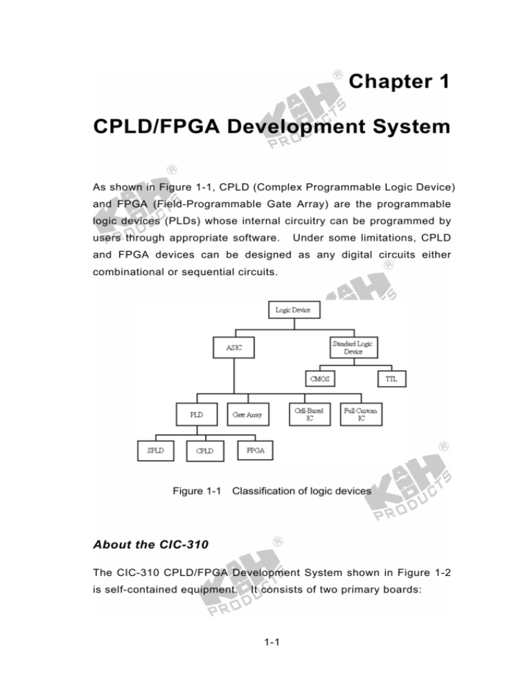
Chapter 1 CPLD/FPGA Development System As shown in Figure 1-1, CPLD (Complex Programmable Logic Device) and FPGA (Field-Programmable Gate Array) are the programmable logic devices (PLDs) whose internal circuitry can be programmed by users through appropriate software. Under some limitations, CPLD and FPGA devices can be designed as any digital circuits either combinational or sequential circuits. Figure 1-1 Classification of logic devices About the CIC-310 The CIC-310 CPLD/FPGA Development System shown in Figure 1-2 is self-contained equipment. It consists of two primary boards: 1-1 1. Development Board EPF8282ALC84 Development Board SN-PLDE2 or EPF10K10LC84 Development Board SN-PLDE3 2. Experiment Board: SN-PLDE3A Figure 1-2 CPLD/FPGA development system We will discuss the Development Board SN-PLDE2 and Experiment Board SN-PLDE3A below. The SN-PLDE3 Development Board will be described in Chapter 9. Development Board SN-PLDE2 The SN-PLDE2 Development Board shown in Figure 1-3 contains an Altera SRAM-based FPGA type EPF8282ALC84-4 (5,000 gate count), AT89C2051 microcontroller, configuration device 24LC64, 89C52 expansion socket, and an RS-232 interface circuit. The AT89C2051 microcontroller is used to load the configuration data to FPGA or SEEPROM devices via RS-232 serial port. Through three 40-pin connectors J1, J2, and J3, the Development Board can easily be connected to a variety of experimental circuits such as the Experiment Board SN-PLDE3A, project board or the user’s circuits on breadboard. 1-2 The RESET button S1 is used to reset the development system. The EXE MODE connector J6 is used to execute a configuration file when a jumper cap is in the position. The next configuration file (displayed on SEEPROM in DNLD window) will be loaded and executed by removing and inserting the jumper cap every time. Connector J5 provides a +5V dc power supply for external circuits. The RS232 connector P1 links the Development Board to personal computer using the supplied RS232 cable. Figure 1-3 SN-PLDE2 development board 1-3 The architecture of Altera’s Flexible Logic Element MatriX (FLEX) devices support five different configuration schemes for loading a design into a single FLEX 8000 device on the circuit board. Chapter 8 for detailed information. Refer to The FLEX 8000 architecture uses SRAM cells to store the configuration data for the device. These SRAM cells must be loaded every time the circuit powers up and begins operation. The process of physically loading the SRAM programming data into the FLEX 8000 device is called configuration. After configuration, the FLEX 8000 device resets its registers, enables its I/O pins, and begins operating as a logic device. reset operation is called initialization. The Together, the configuration and initialization processes are called command mode; normal incircuit device operation is called user mode. When active configuration is selected, the configuration data of FPGA stored in external serial ROM (SROM) or parallel ROM is read and then written to internal SRAM. The CPLD/FPGA Development System reserves the U4 socket for installing Microchip’s SROM type 37LV65 (8 KB). The SROM occupies five FPGA pins: DATA0, nCONFIG, DCLK, CONF_DONE, and nSTATUS. To define the active configuration mode, a jumper cap must be placed in the lowest position of J8. If passive configuration is selected, the configuration data of FPGA is transmitted from a host (personal computer) to FPGA’s configuration RAM via the RS-232 serial communication port. Your CPLD/FPGA Development System CIC-310 is designed to operate in this mode. Therefore two jumper caps are in the upper two positions of J8. Additionally, the configuration data on PC is written into SEEPROM (24LC64, U5) for storing configuration files, and reloading an autoexecutable configuration file to FPGA when the system reboots. The system is equipped with a 24LC64 (8 KB) chip for this purpose 1-4 and can be expanded to 32 KB memory space (4 chips of 24LC64, U5-U8). This configuration mode is defined by the pins NSP, MSEL0, and MSEL1. An AT89C52 microcontroller can be installed in the 89C52 socket to associate with the FPGA device for high-performance designs. Figure 1-4 shows the pin assignments of 89C52. Figure 1-4 Pin assignments of 89C52 socket Through 40-pin connectors J1, J2, J3, the FPGA I/O pins are connected to the various I/O devices on the SN-PLDE3A Experiment Board. The pin assignments of J1-J3 are shown in Figure 1-5. The JP18 on the Experiment Board is used to select the clock signal to FPGA I54 pin from either MTX2 (11.0592 MHz) or P84 (pulser generator SWP4). 1-5 Figure 1-5 J1-J3 connectors Experiment Board SN-PLDE3A The SN-PLDE3A Experiment Board, shown in Figure 1-6, provides several different input and output devices, which are widely used in modern electronic products. These devices include: LEDs, 7- segment and 16-segment displays for display, logic input switches for data input, clock and pulse generators for signal generation. FPGA pins are marked on the Experiment Board panel. 1-6 The Figure 1-6 SN-PLDE3A experiment board 1-7 The Experiment Board is divided into the following sections: 1. Logic Switch Input Section In this section three 8-bit slide switches (S1, S2, and S3) are defined as logic inputs. The pin-out is described in Table 1-1. The circuit diagram of logic input switch is shown in Figure 1-8. Each slide switch is pulled up to V CC level (logic 1) by a 2.2-KΩ resistor when the slide button is placed in the ON position; otherwise it is pulled down to GND level (logic 0) by a 10-KΩ resistor. Figure 1-7 Figure 1-8 Logic switches S1-S3 Logic input switch circuit 1-8 Table 1-1 Logic input switch pin-out S1 FPGA S2 FPGA S3 FPGA S1-1 P01 S2-1 P34 S3-1 P43 S1-2 P02 S2-2 P35 S3-2 P44 S1-3 P03 S2-3 P36 S3-3 P45 S1-4 P04 S2-4 P37 S3-4 P46 S1-5 P06 S2-5 P39 S3-5 P48 S1-6 P07 S2-6 P40 S3-6 P49 S1-7 P08 S2-7 P41 S3-7 P50 S1-8 P09 S2-8 P42 S3-8 P51 The logic state of each switch is indicated by the corresponding logic LED display D1 through D16. 2. Logic LED Display Section There are two sets of 16-LED display as shown in Figure 1-9. The LEDs (D1 through D16) located at the lower right side of the Experiment Board are usually used to indicate the logic state of the logic input switches. indicators if necessary. However, D1-D16 can be used as output In such a case, all of the logic input switch must be in ON position. The other set of 16-LED display is located at the upper right side of the Experiment Board. The LEDs (D17 through D32) are dedicated to indicate the logic state of outputs. These 32 LEDs are buffered by CD40106 ICs as shown in the circuit of Figure 1-10 and the pinout in Table 1-2. 1-9 Figure 1-9 Figure 1-10 Logic LED display Logic LED display circuit 1-10 Table 1-2 Logic LED display pin-out LED FPGA LED FPGA LED FPGA LED FPGA D1 P01 D9 P34 D17 P55 D25 P64 D2 P02 D10 P35 D18 P56 D26 P65 D3 P03 D11 P36 D19 P57 D27 P66 D4 P04 D12 P37 D20 P58 D28 P67 D5 P06 D13 P39 D21 P60 D29 P69 D6 P07 D14 P40 D22 P61 D30 P70 D7 P08 D15 P41 D23 P62 D31 P71 D8 P09 D16 P42 D24 P63 D32 P72 3. 6-DIG Parallel-Serial 7-Segment Display Section The 6-digit parallel-serial 7-segment display, located at the upper side of the Experiment Board, consists of six common-cathode 7segment displays. The segment names and pin assignments are shown in Figure 1-11. The pin-out of the 6-digit 7-segment display is described in Table 1-3. Figure 1-11 Pin assignments of 7-segment display 1-11 Table 1-3 6-digit 7-segment display pin-out DP1 FPGA DP2 FPGA DP3 FPGA SA1 P13 SA2 P22 SA3 P55 SB1 P14 SB2 P23 SB3 P56 SC1 P15 SC2 P24 SC3 P57 SD1 P16 SD2 P25 SD3 P58 SE1 P18 SE2 P27 SE3 P60 SF1 P19 SF2 P28 SF3 P61 SG1 P20 SG2 P29 SG3 P62 SP1 P21 SP2 P30 SP3 P63 SC1* P76 SC2* P77 SC3* P78 DP4 FPGA DP5 FPGA DP6 FPGA SA4 P64 SA5 P34 SA6 P43 SB4 P65 SB5 P35 SB6 P44 SC4 P66 SC5 P36 SC6 P45 SD4 P67 SD5 P37 SD6 P46 SE4 P69 SE5 P39 SE6 P48 SF4 P70 SF5 P40 SF6 P49 SG4 P71 SG5 P41 SG6 P50 SP4 P72 SP5 P42 SP6 P51 SC4* P79 SC5* P08 SC6* P09 Note: *=Common-cathode terminal The common-cathode terminal SC of each digit can be connected to FPGA pin or ground with a jumper cap. When connected to GND, the digit operates in parallel mode (individual mode). If connected to FPGA pin, the digit operates in serial mode (scan mode). In parallel mode, the 8 LED segments (SA-SP) of each digit must be connected to FPGA pins on the left side of each selector (JP8, JP9, JP10, JP11, JP12, JP13) with 8-jumper caps as shown in Figure 112(a). 1-12 To operate in serial mode, the common-cathode terminals SC1 through SC6 must be connected to the FPGA pins P76-P79, P08, and P09, respectively, with jumper caps. The same segments of all digits must be connected in parallel by placing the 8-jumper caps in JP8A through JP13A positions as well as JP8. Figure 1-12(b) shows the positions of jumper caps for serial operation. In such a case, the segments SA through SP are connected to the FPGA pins P13 through P21, and the common-cathode terminals SC1 through SC6 are connected to the FPGA pins P76-P79, P08, and P09, respectively. (a) Parallel mode 1-13 (b) Serial mode Figure 1-12 4. Operating modes of 6-digit 7-segment display Pulser Generator Section This section located at the lower side of the board consists of four debounced push-button switches (SWP1, SWP2, SWP3, and SWP4), which are defined as pulse outputs. Each push-button signal is defined as a logic 1 when pressed; when unpressed it becomes a logic 0. Each of the switches SWP1-SWP4 is a spring-loaded push button switch. When it is pressed and released, the output produces a low-high-low pulse, which is suitable for the clock input of counters or registers. The circuit of pulser generator is shown in Figure 1-13 and the pin-out in Table 1-4. 1-14 Figure 1-13 Table 1-4 5. Pulser generator Pulser generator pin-out Pulser generator FPGA pin SWP1 P81 SWP2 P82 SWP3 P83 SWP4 P84 Clock Generator Section The clock generators RCOSC1 and RCOSC2 are RC oscillators constructed from CD40106 and the associated resistors and capacitors. The RCOSC1 generator can operate in low-frequency range (JP15 LF pins closed) or high-frequency range (JP15 LF pins open). The output frequency is controlled by the HFQ ADJ knob ranging from 5 to 500 KHz. Similarly, the RCOSC2 generator can operate in low-frequency range (JP17 LF pins closed) or highfrequency range (JP17 LF pins open). Its output frequency is adjusted by the LFQ ADJ knob ranging from 0.1 Hz to 20 KHz. RCOSC1 output is connected to FPGA pin 31 (I31) by placing a jumper cap in the I31 position of JP15 and RCOSC2 output is connected to FPGA pin 73 (I73) by placing a jumper cap in the I73 position of JP17. 1-15 The circuits of clock generators and 20-MHz crystal oscillator are shown in Figure 1-14. The output of the crystal oscillator is connected to FPGA pin 12 (I12) for clocking the device. A 20-MHz crystal oscillator is installed in factory, and it can be replaced by another oscillator if a different frequency is needed for different circuit designs. Figure 1-14 6. Clock generators SW and Keyboard Section The 4x4 matrix keyboard can be used in individual and scan modes. 1-16 (a) Individual buttons (b) Circuit Figure 1-15 Matrix keyboard in individual mode 1-17 (a) Scanned keyboard (b) Circuit Figure 1-16 Matrix keyboard in scan mode 1-18 When the matrix keyboard is used in individual mode (8-jumper caps placed in PKI1, PKI2, and PKI3) as shown in Figure 1-15(a), these 16 buttons act as individual buttons and the circuit is shown in Figure 115(b). If the keyboard is used in scan mode (8-jumper caps placed in SCN1, SCN2, and SCN3) as shown in Figure 1-16(a), these 16 buttons act as a 4x4 scanned keyboard and the circuit is shown in Figure 1-16(b). Table 1-5 The keyboard pin-out is described in Table 1-5. Matrix keyboard pin-out Individual Mode Scan Keyboard FPGA Keyboard FPGA Mode SW0 P34 SW8 P43 KIN1 SW1 P35 SW9 P44 KIN2 SW2 P36 SWA P45 KIN3 SW3 P37 SWB P46 KIN4 SW4 P39 SWC P48 SCN1 SW5 P40 SWD P49 SCN2 SW6 P41 SWE P50 SCN3 SW7 P42 SWF P51 SCN4 6. 16-Segment Display Section The 16-segment display is common-cathode type. Its segment names and pin assignments is shown in Figure 1-17. The common- cathode terminal C-SEL must be connected to GND when using the 16-segment display. 1-19 Figure 1-17 16-segment display The pin assignments of the 16-segment display socket JP21 are shown in Figure 1-18. The circuit is shown in Figure 1-19. Figure 1-18 16-segment display socket 1-20 Figure 1-19 16-segment display circuit The 16-segment display pin-out is described in Table 1-6. When using the 16-segment display, 8-jumper caps must be placed in JP8, JP9, JP10 positions and a jumper cap must be in JP23. Table 1-6 16-segment display pin-out 16-segment FPGA 16-segment FPGA A1 P13 (DA1) E2 P23 (DB2) A2 P14 (DB1) G1 P24 (DC2) B1 P15 (DC1) G2 P25 (DD2) B2 P16 (DD1) H1 P27 (DE2) C1 P18 (DE1) H2 P28 (DF2) C2 P19 (DF1) I1 P29 (DG2) D1 P20 (DG1) I2 P30 (DP2) D2 P21 (DP1) DP P63 (DP3) E1 P22 (DA2) C-SEL JP23 (GND) 1-21 7. 5 x 7 DOT LED Section The pin assignments of the 5x7 dot LED are shown in Figure 1-20. The socket for the dot LED (JP22) and the dot selector connector (JP24) are shown in Figure 1-21. Figure 1-22 shows the circuits of JP22 and JP24. Figure 1-20 Figure 1-21 Pin assignments of 5x7 dot LED 5x7 dot LED socket JP22 and dot selector JP24 1-22 Figure 1-22 JP22 and JP24 signals Table 1-7 indicates the pin-out of the 5x7 dot LED. When using the 5x7 dot LED, the 8-jumper caps must be installed in JP8 and JP24. Table 1-7 8. 5x7 dot LED pin-out Dot LED FPGA Dot LED FPGA PA1 P13 C1 P22 PA2 P14 C2 P23 PA3 P15 C3 P24 PA4 P16 C4 P25 PA5 P18 C5 P27 PA6 P19 PA7 P20 LCD 2021 Section The JP20 connector shown in Figure 1-23 is for connecting an external LCD module LCD2021 to the FPGA device. The potentiometer VR1 is used to adjust the contrast of LCD screen and is not installed in factory. If you want to use the function, remove the jumper in VR1 block and install a 10-KΩ potentiometer as shown in Figure 1-23(b). The pin-out is described in Table 1-8. 1-23 (a) LCD2021 connector (b) JP20 circuit Figure 1-23 LCD2021 module Table 1-8 LCD2021 pin-out LCD FPGA LCD FPGA DB0 P13 E P22 DB1 P14 R/W P23 DB2 P15 D/I P24 DB3 P16 LCT DB4 P18 DB5 P19 DB6 P20 DB7 P21 1-24 System Setup Follow the procedure to install the software and hardware of the CIC310 CPLD/FPGA Development System. The system software includes MAX+plus II manager and download manager DNLD programs. Installing Software 1. Put the supplied CPLD/FPGA Development CD-ROM into CD player. The install program auto runs and the MAX+pus II Install window is shown in Figure 1-24. Figure 1-24 2. MAX+pus II Install window Choose the Full/Custom/FLEXIm Server to open the Welcome window shown in Figure 1-25. 1-25 Figure 1-25 3. Welcome window Click on the Next button to open the MAX+plus II License Agreement window as shown in Figure 1-26. Figure 1-26 MAX+plus II License Agreement window 1-26 4. Read the license agreement throughout and then click on Yes button. The Information window is shown in Figure 1-27. Figure 1-27 5. license agreement information Click Next to open the User Information window as shown in Figure 1-28. Figure 1-28 User information window 1-27 6. Type your name and company in the Name and Company fields, respectively. Then click on Next to open the Setup Type window shown in Figure 1-29. Figure 1-29 7. Setup type selection Select Full Installation item and click Next button to open the first Choose Destination Location window shown in Figure 1-30. Figure 1-30 First Choose Destination Location window 1-28 8. Click Next to open the second Choose Destination Location window as shown in Figure 1-31. Figure 1-31 9. second Choose Destination Location window Click Next to open the third Choose Destination Location window as shown in Figure 1-32. Figure 1-32 Choosing destination 1-29 10. Click Next to open the Select Program Folder window as shown in Figure 1-33. Figure 1-33 Select Program Folder window 11. Click Next to open the Start Coping Files window as shown in Figure 1-34. Figure 1-34 Start Coping Files window 1-30 12. Click Next to start installing the software. Once completed, a Question dialog box is shown in Figure 1-35. Figure 1-35 13. Click on Yes button. Question dialog box A readme window will display as shown in Figure 1-36. Figure 1-36 Readme window 1-31 14. Close the windows. Execute C:\Programs\Altera\MAX+plus II v10.1 program to open the MAX+plus II Manager window as shown in Figure 1-37. Figure 1-37 MAX+plus II Manager window 15. Use the Options-License Setup command on the toolbar to open the License Setup window as shown in Figure 1-38. Figure 1-38 License Setup window 1-32 16. Click on the System Info button to view your system information as shown in Figure 1-39. Figure 1-39 System information 17. Write down your C: drive serial number displayed and click OK. Close the License Setup window. Visit Altera web site http://www.altera.com/authcode/index.html and select MAX+plus II Software for Students and Universities item to request free software license. 18. Altera will e-mail a license.dat file to you. C:\maxplus2 folder. Save this file into Open the License Setup window again. Click on Browse and select C:\maxplus2\license.dat as shown in Figure 1-37. Then click on OK button. Setup window 1-33 Close the License Figure 1-40 License setup 19. Copy E:\DNLD3.exe (or DNLD82.exe for WIN2000/NT/XP) file to maxplus2 folder (from My Computer or File Manager). Create DNLD3 shortcut on desktop. 20. The software installation is now completed. 21. Copy E:\EXP folder (this folder includes 3 example folders) files to max2work folder (from My Computer or File Manager). 1-34 Installing Hardware To load the completed designs to FPGA device for emulation, you must link the computer to the CPLD/FPGA Development System CIC310 using RS-232 cable. 1. With all powers off, connect the RS-232 port (COM1 or COM2) on personal computer to the RS-232 connector (P1) on FPGA board SN-PLDE2 using the supplied 9-pin cable. 2. Make sure that the voltage select switch 115V/230V on the bottom panel of CIC-310 is in a correct position. Connect the AC socket on CIC-310 rear panel to the wall outlet via the supplied AC cord. 3. Turn on the power. The power indicator should light up. If not, turn off the power and check the fuse on the rear panel. 4. Proceed to the next Chapter for basic operation of software and hardware. 1-35 1-36
