TECHNICAL ARTICLE
UNDERSTANDING, OPERATING,
AND INTERFACING TO
INTEGRATED DIODE-BASED
RF DETECTORS
Applications Director
for RF Detectors,
Analog Devices, Inc.
| Share on Twitter
| Share on LinkedIn
|Email
Abstract
Because of their fundamental rectifying characteristic, diodes have
been used to generate dc voltages that are proportional to ac and
RF signal levels for as long as there have been diodes. This article
will compare the performance of diode-based RF and microwave
with integrated circuit alternatives. Topics covered will include
transfer function linearity, temperature stability, and ADC interfacing.
Discrete Diode-Based RF Detectors
Figure 1 shows the schematic of a popular diode-based RF detection
circuit. This can be thought of as a simple half wave rectifier with output
filtering. The positive half cycles of the input signal forward bias the
Schottky diode, which in turn charges the capacitor. On the negative half
cycle, the diode reverse biases, causing the voltage on the capacitor to
be held and yielding a dc output that is proportional to the input signal. To
allow this voltage to drop when the input signal decreases or is turned off,
a resistor in parallel to the capacitor provides a discharge path.
RFIN
L1
D1
Figure 2 shows the transfer function of this circuit. Input power is scaled
in dB and output voltage is on a logarithmic vertical scale. Looking at the
25°C transfer function, there are two distinct operating regions on the
curve. The so-called linear region extends from the top end of the input
range (approximately 15 dBm) down to around 0 dBm. This term, linear
region, derives its name from the fact that the output voltage in this region
is roughly proportional to the input voltage.
Below 0 dBm, the so-called square-law region begins. In this region the
output voltage is roughly proportional to the square of the input voltage.
This results in a higher slope on the plot.
Figure 2 also shows the output voltage vs. input power transfer function
of the circuit when the temperature is –40°C and +85°C. This shows
significant deviation at power levels below 0 dBm. This renders the
device unusable in applications where the temperature varies by any
significant amount.
Techniques exist that can be used to somewhat mitigate this temperature
drift. They involve introducing a second reference diode either as part of
the circuit or as a standalone circuit with its own output. The temperature
drift of the reference diode matches that of the primary diode. By a
process of subtraction (either in the analog domain or in the digital
domain based on the circuit structure), some degree of drift cancellation
can be achieved.
+4
VDET
C1
10
Calibration at –28 dBm, –10 dBm, and +8 dBm
+3
R1
1
+2
Error (dB)
Figure 1. A Schottky diode-based RF detector.
101
100
VOUT (V)
0.1
0
–1
10–1
–55°C
–40°C
+25°C
+85°C
+125°C
–2
–3
10–2
–4
–30
10–3
–25
–20
–15
–10
–5
0
+5
+10
0.01
+15
0.001
+20
PIN (dBm)
Figure 3. Output voltage vs. input power and linearity error of an integrated
Schottky diode detector at 25 GHz.
VOUT at +25°C
VOUT at –40°C
VOUT at +85°C
10–4
10–5
–25
+1
Output Voltage (V)
Eamon Nash
–20
–15
–10
–5
0
+5
+10
+15
+20
Input Power (dBm)
Figure 2. Transfer function of a Schottky diode-based RF detector.
Visit analog.com
+25
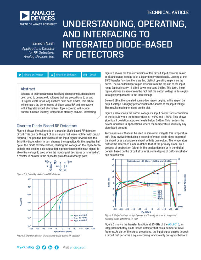
Figure 3 shows the transfer function at 25 GHz of the ADL6010, an
integrated Schottky diode-based detector that has a number of novel
features. As part of the signal processing, the input signal passes through
a circuit that performs a square-rooting function only on signals below a
UNDERSTANDING, OPERATING, AND INTERFACING TO INTEGRATED DIODE-BASED RF DETECTORS
certain power level. The transition point is deliberately set to be equal to
the power level at which the diode transitions from the square law region
to the linear region. As a result of this, the square-law effect of the diode
is canceled out and there is no sign of the two-region transfer function
that is so apparent in Figure 1.
Figure 3 also includes plots showing the transfer function at various
temperatures from –55°C to +125°C. The variation in the transfer
function vs. temperature is also plotted. Using linear regression of the
25°C transfer function as a reference, the error at each temperature
is plotted in dB. As a result of integrated temperature compensation
circuitry and the square-law elimination circuit, we see errors due
to linearity and temperature drift of approximately ±0.5 dB over the
majority of the input range.
ADC Interfacing
While RF and microwave detectors are sometimes used in analog power
control loops,1 it is more common to build a digital power control loop as
shown in Figure 4. In these applications, the output of the power detector
is digitized by an analog-to-digital converter. In the digital domain, the
power level is calculated using the code from the ADC. Once the power
level is known, the system will respond by adjusting the transmitted
power if necessary.
DAC
I/Q Mod
Tx
DAC
FPGA
90° Phase
Shifter
DAC
VGA
PA
Tx
DAC
ADF4151
ADC
Figure 4. A typical digitally controlled RF power control loop.
While the response time of this loop will depend to a small extent on the
response time of the detector, the sampling rate of the ADC and the speed
of the power control algorithm will have a far larger impact.
4
3.5
1000
VOUT HMC1094 Log Amp
VOUT ADL6010 Detector
Bits/dB Resolution—ADL6010
Detector and 5 V, 12-Bit ADC
100
3
2.5
2
1.5
10
1
0.5
0
–60
–40
–20
PIN (dBm)
Figure 5. Comparison of linear-in-dB.
0
Because analog-to-digital converters have a transfer function that is
scaled in bits/voltage, this means that system resolution in terms of
dB-per-bit continually decreases with decreasing input power. The
plot in Figure 5 also shows the bits-per-dB resolution that could be
achieved if the ADL6010 were to drive a 12-bit ADC with a full-scale
voltage of 5 V (this plot is scaled on a logarithmic secondary axis for
ease of viewing). At the low end of the device’s power range, around
–25 dBm, the incremental slope would be approximately 2 bits per
dB, yielding a resolution of approximately 0.5 dB/bit. This suggests
that a 12-bit ADC is adequate to accurately resolve the output of the
ADL6010 over its full range.
By contrast, the transfer function of the HMC1094 log amp in Figure 5 also
shows that it has a constant slope over its linear operation range. This
suggests that a lower resolution ADC (10-bit or possibly even 8-bit) would
be adequate to achieve a resolution that is well below 1 dB.
RF
Power
Detector
4.5
The loop’s ability to measure and precisely set the RF power level is
impacted by a number of factors including the transfer function of the
RF detector and the resolution of the ADC. To better understand this, let’s
take a closer look at the response of the detector. Figure 5 compares the
response at 20 GHz of the ADL6010 diode-based detector to that of a
microwave log amp, the HMC1094. The log amp has a transfer function
that is linear-in-dB, where a 1 dB change in input power always results
in the same voltage change at the output (over the linear input range
of approximately –50 dBm to 0 dBm). In contrast to this, a diode-based
detector such as the ADL6010 has a transfer function that appears
exponential when a dB scale is used on the horizontal axis and a linear
vertical axis is used for output voltage.
As the RF input power increases, the incremental slope in bits/dB increases
steadily to a maximum of approximately 300 bits/dB at the maximum input
power of 15 dBm. This is valuable in an RF power control application
where accuracy is most critical when the system is at its maximum power.
This is a very typical scenario in applications where RF detectors are
used to measure and control the power of a high power amplifier (HPA).
In applications where power is often being controlled to prevent the HPA
from overheating, high resolution power measurement at max power is of
great value.
1
+20
Detector ADC Resolution (Bits/dB)
2
RF Detector Output Voltage (V)
Figure 6 shows an application circuit where the ADL6010 has been
interfaced to the AD7091, a 12-bit precision ADC that can sample at up to
1 MSPS. The ADC has an internal 2.5 V reference that sets the full-scale
input voltage. Because the ADL6010 detector can reach a maximum
voltage of approximately 4.25 V, a simple resistor divider is used to
scale this voltage down so that it never exceeds 2.5 V. This scaling can
be implemented without the need for an op amp buffer. The achievable
resolution in terms of dB-per-bit at the bottom end of the input power range
is similar to the example above (that is, approximately 0.5 dB-per-bit).2
Visit analog.com 5V
VPOS
ADL6010 Detector
Maximum
Output = 4 V
5V
Input Range:
0 V to 2.5 V
VDD
RFCM
RF Input
Power
RFIN
RFCM
Analog
Signal
Processor
VOUT
VIN
200 Ω
340 Ω
AD7091R
12-Bit,
1 MSPS ADC
GND
Comm
Figure 6. Interfacing an integrated microwave power detector to a precision ADC.
Conclusions
Integrated RF and microwave detectors offer a number of benefits
when compared to discrete implementations. Integrated temperature
compensation circuitry offers an out-of-the-box output voltage that is
stable to within around ±0.5 dB over a wide temperature range. The use
of an internal square-rooting function effectively eliminates the squarelaw characteristic at low input power levels. This results in a single
linear transfer function, making device calibration easier. The buffered
output of the integrated detector can drive ADCs directly without any
concerns that the loading will affect the computational accuracy. Care
does need to be taken in choosing and dimensioning the ADC so that
adequate bits/dB can be achieved at low input powers.
References
1
CN-0050 Circuit Note. Stable, Closed-Loop Automatic Power Control for
RF Applications. Analog Devices, Inc., 2010.
2
CN-0366 Circuit Note. A 40 GHz Microwave Power Meter with a Range
from −30 dBm to +15 dBm. Analog Devices, Inc., 2014.
Online Support
Community
Engage with the Analog Devices
technology experts in our online
support community. Ask your
tough design questions, browse
FAQs, or join a conversation.
ez.analog.com
SPI
3
Analog Devices, Inc.
Worldwide Headquarters
Analog Devices, Inc.
Europe Headquarters
Analog Devices, Inc.
Japan Headquarters
Analog Devices, Inc.
Asia Pacific Headquarters
Analog Devices, Inc.
One Technology Way
P.O. Box 9106
Norwood, MA 02062-9106
U.S.A.
Tel: 781.329.4700
(800.262.5643, U.S.A. only)
Fax: 781.461.3113
Analog Devices, Inc.
Wilhelm-Wagenfeld-Str. 6
80807 Munich
Germany
Tel: 49.89.76903.0
Fax: 49.89.76903.157
Analog Devices, KK
New Pier Takeshiba
South Tower Building
1-16-1 Kaigan, Minato-ku,
Tokyo, 105-6891
Japan
Tel: 813.5402.8200
Fax: 813.5402.1064
Analog Devices
5F, Sandhill Plaza
2290 Zuchongzhi Road
Zhangjiang Hi-Tech Park
Pudong New District
Shanghai, China 201203
Tel: 86.21.2320.8000
Fax: 86.21.2320.8222
©2015 Analog Devices, Inc. All rights reserved. Trademarks and
registered trademarks are the property of their respective owners.
Ahead of What’s Possible is a trademark of Analog Devices.
TA13826-0-11/15
analog.com
