PHYSICS 327 ______ 4/97
advertisement
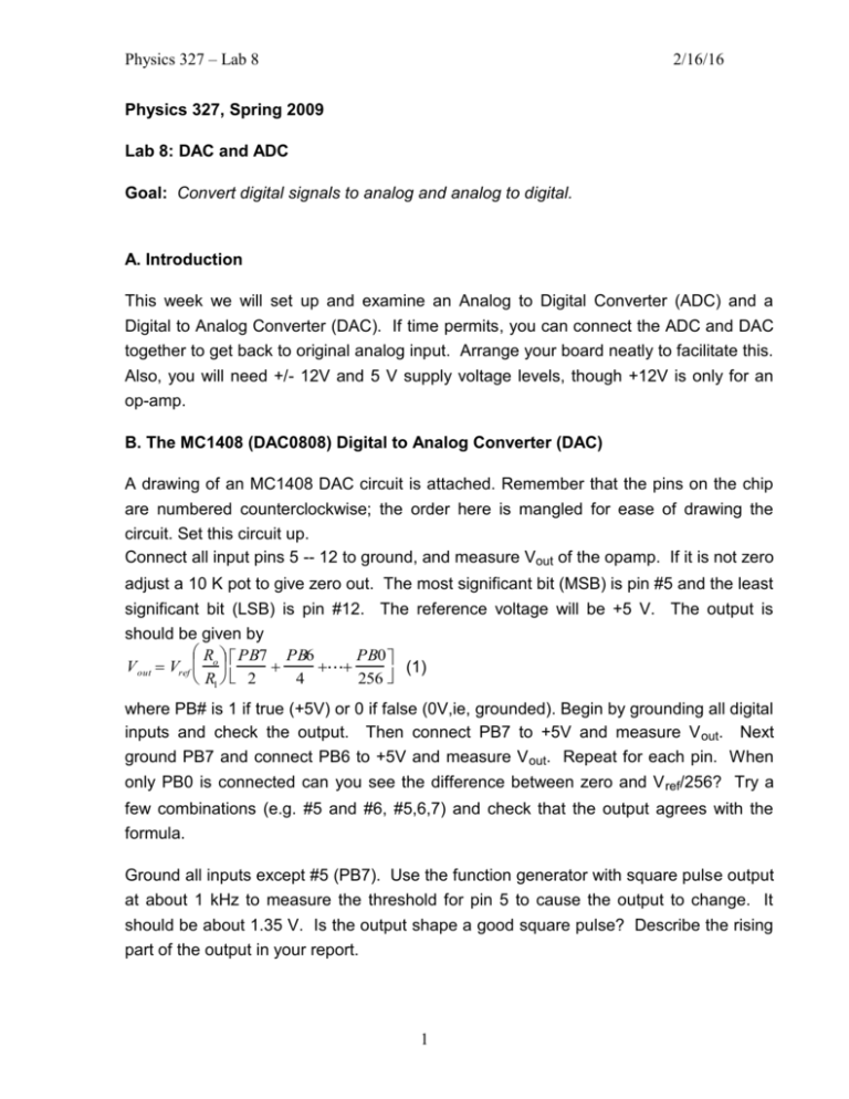
Physics 327 – Lab 8 2/16/16 Physics 327, Spring 2009 Lab 8: DAC and ADC Goal: Convert digital signals to analog and analog to digital. A. Introduction This week we will set up and examine an Analog to Digital Converter (ADC) and a Digital to Analog Converter (DAC). If time permits, you can connect the ADC and DAC together to get back to original analog input. Arrange your board neatly to facilitate this. Also, you will need +/- 12V and 5 V supply voltage levels, though +12V is only for an op-amp. B. The MC1408 (DAC0808) Digital to Analog Converter (DAC) A drawing of an MC1408 DAC circuit is attached. Remember that the pins on the chip are numbered counterclockwise; the order here is mangled for ease of drawing the circuit. Set this circuit up. Connect all input pins 5 -- 12 to ground, and measure Vout of the opamp. If it is not zero adjust a 10 K pot to give zero out. The most significant bit (MSB) is pin #5 and the least significant bit (LSB) is pin #12. The reference voltage will be +5 V. The output is should be given by R PB7 PB6 PB0 V out Vref o (1) R1 2 4 256 where PB# is 1 if true (+5V) or 0 if false (0V,ie, grounded). Begin by grounding all digital inputs and check the output. Then connect PB7 to +5V and measure V out. Next ground PB7 and connect PB6 to +5V and measure V out. Repeat for each pin. When only PB0 is connected can you see the difference between zero and V ref/256? Try a few combinations (e.g. #5 and #6, #5,6,7) and check that the output agrees with the formula. Ground all inputs except #5 (PB7). Use the function generator with square pulse output at about 1 kHz to measure the threshold for pin 5 to cause the output to change. It should be about 1.35 V. Is the output shape a good square pulse? Describe the rising part of the output in your report. 1 Physics 327 – Lab 8 2/16/16 C. The ADC0809 Analog to Digital Converter (ADC) A drawing of a 0809 ADC circuit is shown on the next page. Set this circuit up. Initially, use a 500 kHz square pulse from the function generator as input to the clock. Clock input voltage levels should extend at least from 0 to 5 V. The inputs must be POSITIVE. Negative voltages can damage the ADC. Before applying the clock signal to the ADC, display the clock signal on the scope(dc couple) and check with instructor. Apply a DC voltage of about 0.5 V to IN0, pin 26. If the chip does not convert when you turn power on, momentarily apply +5 V to the start pin, then leave it open. Connecting EOC (end of conversion) to start should cause the chip to continuously convert once it has been started. Does the digital output make sense? Remember the output is binary, ranging from about 0 V to Vref, and from 0 to 11111111. Repeat this for at least four other voltages to check linearity. Also adjust one voltage slightly to see if you can determine what voltage change corresponds to a change of one unit in the LSB and explain how you did this in your lab report. Measure the conversion time of the ADC. Disconnect EOC from START. Use a 555 timer to put a ~1 kHz square pulse into START, and monitor this on the oscilloscope. Also monitor EOC on the oscilloscope. The time difference between HILO of the start and LOHI of EOC is the conversion time. Redo this exercise at a clock frequency of 200 kHz. Do you find any simple relationship between clock frequency and conversion time? Can you explain it? D. Analog to Digital to Analog (optional) Reset the ADC for continuous conversion. Use the 555 at an output frequency to a few hundred kHz as the clock input. Be careful: it does not give out a good square pulse at too high a frequency. Reset the function generator to a few hundred Hz triangular pulse, with a DC offset such that the signal is always positive, and connect to IN0. Hook up the ADC outputs to the appropriate DAC inputs. Compare on the scope the input triangular wave with the DAC / opamp output triangular wave. Show and explain the differences in your lab report. What happens as you increase the input triangle frequency? 2 Physics 327 – Lab 8 2/16/16 3
