PSPICE HANDOUT BASIC DIGITAL LOGIC GATES Page 1
advertisement
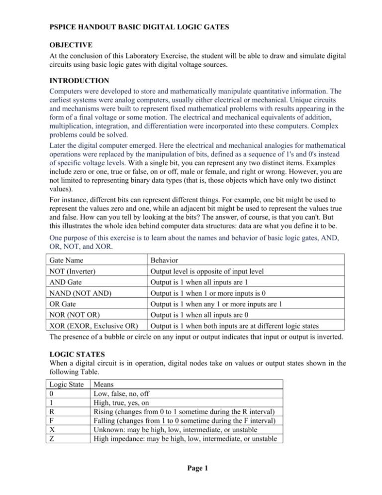
PSPICE HANDOUT BASIC DIGITAL LOGIC GATES OBJECTIVE At the conclusion of this Laboratory Exercise, the student will be able to draw and simulate digital circuits using basic logic gates with digital voltage sources. INTRODUCTION Computers were developed to store and mathematically manipulate quantitative information. The earliest systems were analog computers, usually either electrical or mechanical. Unique circuits and mechanisms were built to represent fixed mathematical problems with results appearing in the form of a final voltage or some motion. The electrical and mechanical equivalents of addition, multiplication, integration, and differentiation were incorporated into these computers. Complex problems could be solved. Later the digital computer emerged. Here the electrical and mechanical analogies for mathematical operations were replaced by the manipulation of bits, defined as a sequence of 1's and 0's instead of specific voltage levels. With a single bit, you can represent any two distinct items. Examples include zero or one, true or false, on or off, male or female, and right or wrong. However, you are not limited to representing binary data types (that is, those objects which have only two distinct values). For instance, different bits can represent different things. For example, one bit might be used to represent the values zero and one, while an adjacent bit might be used to represent the values true and false. How can you tell by looking at the bits? The answer, of course, is that you can't. But this illustrates the whole idea behind computer data structures: data are what you define it to be. One purpose of this exercise is to learn about the names and behavior of basic logic gates, AND, OR, NOT, and XOR. Gate Name Behavior NOT (Inverter) Output level is opposite of input level AND Gate Output is 1 when all inputs are 1 NAND (NOT AND) Output is 1 when 1 or more inputs is 0 OR Gate Output is 1 when any 1 or more inputs are 1 NOR (NOT OR) Output is 1 when all inputs are 0 XOR (EXOR, Exclusive OR) Output is 1 when both inputs are at different logic states The presence of a bubble or circle on any input or output indicates that input or output is inverted. LOGIC STATES When a digital circuit is in operation, digital nodes take on values or output states shown in the following Table. Logic State 0 1 R F X Z Means Low, false, no, off High, true, yes, on Rising (changes from 0 to 1 sometime during the R interval) Falling (changes from 1 to 0 sometime during the F interval) Unknown: may be high, low, intermediate, or unstable High impedance: may be high, low, intermediate, or unstable Page 1 PSPICE HANDOUT BASIC DIGITAL LOGIC GATES V1 V2 TD PW Minimum Voltage Maximum Voltage Time Delay from 0 to rise Pulse Width time at V2 TR Rise Time from 10% V1 to 90% V2 TF Fall Time from 90% V2 to 10% V1 PER Period time for 1 cycle Duty Cycle PW/PER * 100% DIGITAL VOLTAGE SOURCES As mentioned earlier, digital systems are more concerned with the logic state of an output that defined as logic 1 or 0 rather than a specific voltage. While there are different logic families of Integrated Circuits and they have different voltage and current specifications, these considerations are beyond the scope of this course, and are not considered when running PSpice simulations. Digital or mixed Analog/Digital simulations accept inputs and provide outputs as logic states. Digital input signals (source voltages) are available from a number of different defined parts. We will use STIM1 in these simulations STIMn part properties Property Description WIDTH Number of output signals (nodes). FORMAT Sequence of digits defining the number of signals corresponding to a digit in any <value> term appearing in a COMMANDn property definition. Each digit must be either 1, 3, or 4 (binary, octal, hexadecimal, respectively); the number of all digits in FORMAT must equal WIDTH. IO_MODEL I/O model describing the stimulus’ driving characteristics. IO_LEVEL Interface subcircuit selection from one of the four analog/digital subcircuits provided with the part’s I/O model. DIG_PWR Digital power pin used by the interface subcircuit. DIG_GND Digital ground pin used by the interface subcircuit. TIMESTEP Number of seconds per clock cycle or step. COMMAND1 - Stimulus transition specification statements including time/value pairs, labels, COMMAND16 and conditional constructs. The Time/Value pairs entered are space delimited. Page 2 PSPICE HANDOUT BASIC DIGITAL LOGIC GATES Using STIM1, STIM4, STIM8 and STIM16 parts The STIMn parts have a single pin for connection. STIM1 is used for driving a single bit. STIM4, STIM8 and STIM16 drive buses that are 4, 8 and 16 bits wide, respectively. The properties for all of these parts are the same as those shown in the Table below. When placed, you must connect each part to the wire or bus of the corresponding radix (number of bits). Typically, each COMMANDn property contains only one command line. It is possible to enter more than one command line per property by placing \n+ between command lines in a given definition. (The n must be lower case and no spaces between characters; spaces may precede or follow the entire key sequence.) Typically, we will use the STIM1 Part Reference for digital Stimulus, and only modify the Commandn values in the Property Editor. In the Property Editor, we will define the time in seconds from t = 0 and the logic state at that time (either 1 or 0) for each COMMANDn entry. When entering the commandn values, they are entered as time, a space, and the logic level entered as a binary value (0 or 1). We will use up to three different STIM1 sources. PSpice will sequentially number them from DSTIM1 through DSTIM3. Do not omit the m from the time value as it contains the order of magnitude. Also, if you inadvertently enter the next COMMAND time with a value less than the previous entry, you will receive an error message when you attempt to run a simulation. The COMMANDn times and logic levels are listed in the table below. DSTM1 DSTM2 DSTM3 Command1 0s 0 0s 0 0s 0 Command10 9m 1 18m 1 4.5m 1 Command11 10m 0 20m 0 5m 1 Command12 11m 1 22m 1 5.5m 0 Command13 12m 0 24m 0 6m 1 Command14 13m 1 26m 1 6.5m 0 Command15 14m 0 28m 0 7m 1 Command16 15m 1 30m 1 7.5m 0 Command2 1m 1 2m 1 0.5m 1 Command3 2m 0 4m 0 1m 0 Command4 3m 1 6m 1 1.5m 1 Command5 4m 0 8m 0 2m 0 Command6 5m 1 10m 1 2.5m 1 Command7 6m 0 12m 0 3m 0 Command8 7m 1 14m 1 3.5m 1 Command9 8m 0 16m 0 4m 0 Note: Grounds are not required when using digital stimuli and digital integrated circuits. They are defined and connected as part of the part. We will not modify these grounds. However, it is possible that when we connect analog devices to digital circuits, we may have to connect power or ground to these devices. Page 3 PSPICE HANDOUT BASIC DIGITAL LOGIC GATES PROCEDURE Place your PSpice work disk in the drive and run Capture. The component part references (Gates and STIM1) and Properties are: OR 7432 NOR 7402 AND 7411 NAND 7410 NOT 7404 DSTM1 DSTM2 DSTM3 1. Create a New Blank Project named lab1a. Draw a digital circuit as follows: Enter an OR gate, part reference 7432 with the output node (the single pin) facing to the right. Enter DSTM1 right 1 inch to the left and ½ inch above input pin 1 of the 7432. DCL on DSTM1 and enter the Commandn values from the table above. Enter DSTM2 right 1 inch to the left and ½ inch below input pin 2 of the 7432. DCL on DSTM2 and enter the Commandn values from the table above. Connect wires from the as necessary to connect the DSTM1 to pin 1 of the 7432, and DSTM2 to pin 2. Add a wire about 1 inch long from the output pin3 to the right and stop. Add the Net Alias A to the node of DSTM1 Add the Net Alias B to the node of DSTM2 Add the Net Alias Q to the output node of the 7432 Create a New Simulation Profile named lab1a for Time Domain (Transient) Analysis using the following: Run Time is 8m Start Saving after 0 Maximum Step Size 0.8m CL on OK Enter ground referenced voltage probes in order to nodes A, B, and Q. Your circuit should be similar to the graphic on the right. Run the Simulation. In the top left corner, DCL on TM1:Pin1 From the list on the left, DCL on A DCL on TM2:Pin1 From the list on the left, DCL on B Your output should be now similar to the following graphic where A and B are the input waveforms, and Q is the output waveform. Note: in the previous instructions, it was not necessary to change TM1 and TM2 to A and B. However, if we print the output and look at it later, the output waveform would be easier to interpret, especially if the schematic was not available. The reason is beginning letters of the alphabet are typically used for digital inputs, and Q is commonly used for digital outputs in Boolean Equations and Truth Tables. By changing the labels, we can readily create a truth table from the waveform diagram, which would help us identify the logic function or Boolean Equation for the circuit. Page 4 PSPICE HANDOUT BASIC DIGITAL LOGIC GATES 2. 3. 4. Create a New Project named lab1b based on the project lab1a. If you do this, you will not have to reenter the DSTM values. Modify the digital circuit as follows: Delete the 7432 and enter a 7402. The remainder of the circuit and instructions for step 1 are the same. Create a New Simulation Profile named lab1b for Time Domain (Transient) Analysis using the simulation time parameters from step 1. After you run the simulation, change TM1:Pin1 to A and TM2:Pin1 to B Create a New Project named lab1c based on the project lab1a. Modify the digital circuit as follows: Delete the 7432 and enter a 7411. Notice this is a 3-input gate. Enter DSTM3 right 1 inch to the left and below input pin 13 of the 7411. DCL on DSTM2 and enter the Commandn values from the table above. Enter the Net Alias C to the new node. The remainder of the circuit and instructions from step 1 are the same. Create a New Simulation Profile named lab1c for Time Domain (Transient) Analysis using the simulation time parameters from step 1. After you run the simulation, change the input labels to A, B, and C if necessary. Create a New Project named lab1d based on the project lab1c. Modify the digital circuit as follows: Delete the 7411 and enter a 7410. Notice this is a 3-input gate. The remainder of the circuit and instructions from step 3 are the same. Create a New Simulation Profile named lab1d for Time Domain (Transient) Analysis using the simulation time parameters from step 3. After you run the simulation, change the input labels to A, B, and C if necessary. Page 5 PSPICE HANDOUT BASIC DIGITAL LOGIC GATES A NOT gate performs the digital function of Complementation (or negation). This means that whatever digital logic level is present on the input, the opposite logic level is present on the output. If the input is Q, the output is QBAR or Q which is stated as NOT Q 5. Create a New Project named lab1e based on the project lab1d. Modify the digital circuit as follows: Add a NOT gate, a 7404, to the output with the Net Alias Q Add a wire about 1 inch long to the output of the 7404. Add a Net Alias QBAR to the node. Create a New Simulation Profile named lab1e for Time Domain (Transient) Analysis using the simulation time parameters from step 1. After you run the simulation, change TM1:Pin1 to A and TM2:Pin1 to B if necessary. Assemble the hard copies in the proper order with a cover sheet on top, and submit to your instructor. Page 6
