Design Flow for Digilent XC95 Boards (using Xilinx XC95108 CPLDs)
advertisement
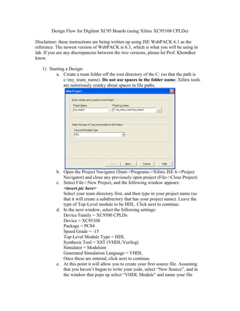
Design Flow for Digilent XC95 Boards (using Xilinx XC95108 CPLDs) Disclaimer: these instructions are being written up using ISE WebPACK 6.1 as the reference. The newest version of WebPACK is 6.3, which is what you will be using in lab. If you see any discrepancies between the two versions, please let Prof. Khondker know. 1) Starting a Design: a. Create a team folder off the root directory of the C: (so that the path is c:\my_team_name). Do not use spaces in the folder name; Xilinx tools are notoriously cranky about spaces in file paths. b. Open the Project Navigator (Start->Programs->Xilinx ISE 6->Project Navigator) and close any previously open project (File->Close Project) c. Select File->New Project, and the following window appears: <insert pic here> Select your team directory first, and then type in your project name (so that it will create a subdirectory that has your project name). Leave the type of Top-Level module to be HDL. Click next to continue. d. In the next window, select the following settings: Device Family = XC9500 CPLDs Device = XC95108 Package = PC84 Speed Grade = -15 Top-Level Module Type = HDL Synthesis Tool = XST (VHDL/Verilog) Simulator = Modelsim Generated Simulation Language = VHDL Once these are entered, click next to continue. e. At this point it will allow you to create your first source file. Assuming that you haven’t begun to write your code, select “New Source”, and in the window that pops up select “VHDL Module” and name your file appropriately. Make sure “Add to project” is checked, and click “Next”. It will now allow you to define your interface (this is what will go in the created file’s entity statement; if you would rather do this later, just click “Next”). It will then ask you to confirm; click “Finish” and it creates the file. Once the file is created, click “Next”. f. If you have already written some parts of your design in VHDL and would now like to include them in your project, you can do that using the “Add Source” button. Once you are done adding files click “Next” g. Finally it will ask you to confirm your project settings, click “Finish”. 2) Entering and Programming a Design Your workspace should look like the following window: In the upper left corner is your “Source Browser”. This will automatically create a hierarchal view of your source files as entities in one file are included as components in another. Right below it is the “Processes” window; this is where you compile, add pin assignments, synthesis and fit your design, as well as view your results and program your CPLD. To the right of these is your text editing window, tabbed at the bottom. Finally at the bottom of the screen is your console window, where you can see the messages returned by each of the tools used in the “Processes” window. a. Enter your VHDL as you normally would. You can check to see if a particular file will compile by clicking on the file in the Source Browser and then selecting Check Syntax (under Implement Design -> Synthesize – XST) b. Once you have completed your design and are ready to fit and program, click your top-level VHDL file in the Source Browswer (very important) and then right click on “Implement Design” and select properties. From there check the following settings: i. Under the Synthesis tab: 1. Optimization Goal -> Area ii. Under the Fitting tab: 1. Implementation Template -> Optimize Density 2. Use Location Constraints -> Always 3. Use Global Clocks/OEs/Set-Reset -> all checked 4. Logic Optimization -> Density 5. Collapsing Input Limit -> 36 6. Collapsing Pterm Limit -> Set to 5 if you really want to know how many macrocells your design will take during fitting, otherwise leaving at 90 is fine. Click OK to close the Properties window. c. Run the processes “Synthesize – XST” (if there are errors here it is probably VHDL coding errors) and “Translate”. At this point you are ready to assign pins by running the “Assign Package Pins” process in the User Constraints file. It will ask you if you want to create a UCF file, click “Yes”. d. Another program called PACE will now open up. In the lower-right window, you can assign inputs and outputs from your top-level entity to pins by typing “p<pin number>” under the Loc column for each I/O name. Once you have entered a pin for each I/O signal, save your changes and close PACE. e. Make sure the top-level source is still selected in the source browser, and then run the “Fit” process. At this point you will be told how many equations are needed to create your design – if you have the Collapsing Pterm Limit set to 5, this will equal how many macrocells your design is using. f. If your design compiles successfully, it is time to program. Connect the parallel port cable to the parallel port (pretty sure it wants the PP on the motherboard) on the PC and the XC95 board, and plug the XC95 board power in. Next, run “Configure Device (iMPACT)” i. A window will pop up that you can click Next through until it closes. It should then search for your device. If it sees it, an icon in the white window should pop up with “xc95108” written below it. If it says “UNKNOWN”, more than one icon pops up, or the software doesn’t detect anything, first make sure that your board is on and plugged in to the computer properly. If it still doesn’t work, ask for help. ii. Once the device is found, it will ask you to give it the name of the programming file. This file will be my_project.jed, where my_project is what you named your project back in step 1c. iii. Right-click on the device icon, and select Program. A window will pop up; make sure “Erase Before Programming” and “Verify” are checked, and start the programming. This will take 15-20 seconds so be patient. Once the task bar has run to the end and “Programming Successful!” pops up, you can unplug the device from the computer (if you wish) and test your design.
