Digital Electronics Dr. Pogo Lab #1 Page 1 of 8 Overview of Digital
advertisement

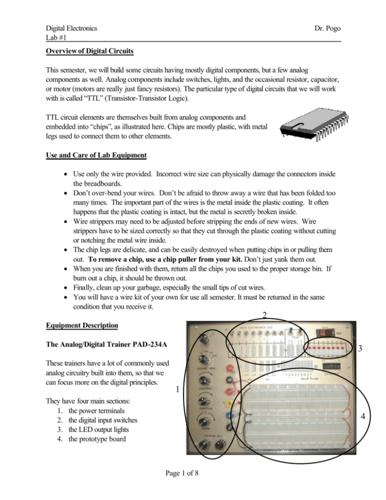
Digital Electronics Lab #1 Dr. Pogo Overview of Digital Circuits This semester, we will build some circuits having mostly digital components, but a few analog components as well. Analog components include switches, lights, and the occasional resistor, capacitor, or motor (motors are really just fancy resistors). The particular type of digital circuits that we will work with is called “TTL” (Transistor-Transistor Logic). TTL circuit elements are themselves built from analog components and embedded into “chips”, as illustrated here. Chips are mostly plastic, with metal legs used to connect them to other elements. Use and Care of Lab Equipment • Use only the wire provided. Incorrect wire size can physically damage the connectors inside the breadboards. • Don’t over-bend your wires. Don’t be afraid to throw away a wire that has been folded too many times. The important part of the wires is the metal inside the plastic coating. It often happens that the plastic coating is intact, but the metal is secretly broken inside. • Wire strippers may need to be adjusted before stripping the ends of new wires. Wire strippers have to be sized correctly so that they cut through the plastic coating without cutting or notching the metal wire inside. • The chip legs are delicate, and can be easily destroyed when putting chips in or pulling them out. To remove a chip, use a chip puller from your kit. Don’t just yank them out. • When you are finished with them, return all the chips you used to the proper storage bin. If burn out a chip, it should be thrown out. • Finally, clean up your garbage, especially the small tips of cut wires. • You will have a wire kit of your own for use all semester. It must be returned in the same condition that you receive it. 2 Equipment Description The Analog/Digital Trainer PAD-234A These trainers have a lot of commonly used analog circuitry built into them, so that we can focus more on the digital principles. 3 1 They have four main sections: 1. the power terminals 2. the digital input switches 3. the LED output lights 4. the prototype board 4 Page 1 of 8 Digital Electronics Lab #1 Dr. Pogo 1. The Power Terminals Ground, +5 Volts power, Signal Generator, and clock TTL chips are powered by +5 Volts. This can be confusing since the high (or logical 1) signals are also at +5 Volts. However, you should keep the concept of a power line and a signal line distinct in your mind when building circuits. Although both lines may have the same voltage on them, they may carry very different currents. You can never power a chip with a signal output, even if it is “high”. A device is not actively powered unless it is connected to both a power and a ground. The symbol for ground is shown on the right. You’ll see it a lot. On the power connector strip shown just to the right, there are six terminals. The third terminal from the top (red) is the +5 Volt power source terminal (also called VCC). Every chip must be connected to this power source before it will work. The bottom terminal (black) is the ground wire of the power supply, and it must also be connected to every chip. The top-most terminal (red, marked “CLK”) is the output point for a “clock” signal. The clock signal oscillates between 0 and 5 volts (a “square wave”), and can be set to various frequencies using the knobs. We will use this clock later in the semester. The yellow (+12 V) and blue (−12V) connectors are power supplies for use with various analog components. To use these to power an analog device, you still need to also connect the device to a ground. The frequency range of the clock is determined by the second knob from the top. For “Ground” example, 10,000 pulses per second is one range setting (10K). The third knob from the top adjusts the frequency of square pulses within that specified range. Note the potentially confusing labeling: the label is below each knob, so that the knobs just described are the “COARSE FREQ” and “FINE FREQ” ones. The top knob should always be at the right-most setting (square wave) , and the bottom two knobs will never make any difference for anything that we do. 2. TTL input devices There are two types of switches on the trainer: momentary switches, and single-pole double throw (SPDT) switches. The output of each switch is either 0 or +5 volts at all times. There are 8 SPDT's and 2 momentary switches. We’ll discuss the difference between them later; for now, use the SPDT’s (the eight switches). SPDT Switches Page 2 of 8 Momentary Switches Digital Electronics Lab #1 Dr. Pogo 3. LED output display devices TTL outputs can be displayed on a bank of 8 red LEDs (Light Emitting Diodes). Although I’m calling then LEDs, they include several other components to make them work with digital signals. The PAD-234A trainer automatically converts digital TTL signals into a similar analog signal capable of powering these lights. They will light up whenever the input is high, and they will remain dark whenever their input is low (or, of course, when they are not connected). 4. Prototype board (or “breadboard”) Prototype boards are a convenient way to connect electrical components together. There are more reliable and/or permanent methods (e.g., soldering), but they require more work. The proto-boards are constructed in such a way that when a wire is inserted into a hole, it is connected to anything in the same “bank” of holes (by wires hidden under the board). The line drawing shows how the banks are laid out. In a circuit, unless something has gone horribly wrong, two things that are connected by a wire have the same voltage. So, if you connect a wire from the +5V power terminal to any other device, that device will also be at +5V. The other device can be an LED, or a set of locations on the protoboard. Similarly, items connected to ground by wires should all be at +0V. On the protoboard shown, there are 8 horizontal banks of holes; 4 are adjacent to red lines, and 4 are adjacent to blue lines. Notice that we added red wires along the edge of the breadboard to connect all 4 red banks together, and black wires to connect all 4 blue banks together. In addition, a single black wire connects one of the blue banks to ground, and a single red wire connects one of the red banks to the +5V terminal (these wires are more easily seen in the first image of the PAD-234A on page 1). When you are done with a circuit, you should remove all the components you have added, but leave these power wires connected to the power banks. Since all of the holes in any horizontal bank are connected together by wires underneath the protoboard, every one of the holes adjacent to a red line is also now connected to +5V. Using these holes, you can connect a large number of devices to +5V without crowding. Page 3 of 8 Digital Electronics Lab #1 Dr. Pogo Chips are placed on the breadboard so that each metal leg goes into a hole. Each chip must straddle one of the troughs, as shown here. All 5 holes perpendicular to the trough are connected by wires hidden in the breadboard, but are not connected across the trough. This way, you can connect wires to the chip legs easily, by just connecting the wire to one of the other 4 holes in the same column as the chip leg (“pin”) you are interested in. Chips are always laid so that the semi-circular notch is on the left (or, equivalently, so that the words are readable). In order to keep track of which wire does what, good circuits use color coding. A universal rule, which you are required to observe in this class, is to use only red wires for power (+5V), and use only black wires for ground (+0V). Do not use red or black wires for other purposes. The electric current in these “power” wires will be higher than in other wires we use (but still not dangerously high). All other wires are called “logic” or “signal” wires, and for this course, signal wires will carry virtually zero current. Chips 14 The TTL chips that we are using usually have 14 or 16 pins. The chip is usually viewed as shown here, with the notch (or circular depression) on the left. The legs are numbered from 1 to 14 (or to 16) counterclockwise, starting in the lower left corner. The name can be hard to read for two reasons: 1. It is faded. But, you’re young and you have good eyes. 2. It contains extraneous information. For example, what I call a “7400” chip might actually be called “DV74ALS00N”. Basically, you usually just ignore the letters. Name Info 1 Be sure your chip is pushed down all the way into the breadboard, without accidentally bending the legs. Digital Volt-Ohm Meter (or Multimeter) The Digital Multimeter is a measurement and display device (we won't use it very much, because its strength is with analog circuits). It can measure current, voltage, or resistance, and display the value on an LCD. In this lab you will use this instrument to primarily measure voltage. This tool will help you locate short-circuits and overloads, which can otherwise be frustratingly hard to find. Since voltages in TTL circuits should always be 0V or +5V, if the multimeter tells you that a voltage is +2.8V, you know you have a problem. To measure voltage, make sure the left tan rectangular button labeled “AC” and “DC” is not pressed in, press in the tan button marked “V”, and press in the rightmost brown button, marked "AUTO". Using thick wires with plugs on the end, connect one end of a black wire to the black common terminal Page 4 of 8 Digital Electronics Lab #1 Dr. Pogo (“COM”), and the other end to the ground post of the power supply on the trainer. Connect a similar red wire to the "VOLTS OHMS mA" terminal. You are now ready to make measurements. Simply touch the free end of the red wire to the point where you want to examine the voltage. Since the plugs are fat and the breadboard holes are small, you may find that you want to add an alligator clip to the plug, and grab a small wire with the alligator clip. The Logic Probe The logic probe is another measuring device. When your circuit has problems, this tool is usually the only way to discover them. It allows you to examine whether a TTL signal is “High” or “Low”. If the signal is high, the corresponding LED will light, and if the signal is low, the other LED will light. I cannot stress enough how useful this tool is for debugging! If the probe is unconnected to anything, or is connected to a voltage somewhere between 0V and +5V, neither LED will light. So, it gives less information than the multimeter. If the signal is in between 0 and 5 volts, for example 3 volts, neither LED should light. If you want to know the exact voltage, you need to use a voltmeter (or multimeter). The Logic Probe must be powered by connecting its red alligator clip to +5v and its black clip to ground. Set the switches to the “PULSE” and “DTL/TTL” or “TTL” positions. Note that on some of our probes, the high and low LEDs are colored red and green respectively, for even easier reading. Since it is so easy to use, and since we usually want to know logic levels rather than voltages… The logic probe is your number-one debugging device! I will not help you with your projects if you don’t already have an active logic probe connected. If you have a problem, and you haven’t used your logic probe, then you are not even trying. Page 5 of 8 Digital Electronics Lab #1 Dr. Pogo Experimental Procedure Part A: Power, Switches, and LEDs A1. Use a single wire to connect an SPDT switch to an LED and examine the output. Which way is the switch when the LED is lit? Check the output of the switch with the logic probe, then check it with the multimeter. How close is the “high” signal to +5V? How close is the “low” to 0V? Record your answers on the worksheet at the bottom of this document. A2. Examine the two sets of contacts beneath a momentary switch. How do these contacts differ? The switch is “off” if you are not touching it. Does the number printed above each column indicate the “on” value or does it indicate the “off” value? A3. Connect the clock output to an LED, and adjust the frequency. How does the LED appear at frequencies less than 5 Hz? At frequencies larger than 1000 Hz? Do the same with a logic probe instead of an LED. At what frequency does the logic probe become ineffective? Part B: Some TTL Chips Vcc The schematic shown uses a 7408 chip, which contains 4 identical “gates”. Each gate has two inputs (“A” and “B”), and one output (“Y”), as seen in the handout from class. We’re only going to use the first gate for now. In addition to these 12 terminals, the chip also has 1 terminal for power, and 1 for ground. These power pins are shared by all 4 gates. Recall that VCC (see pin 14) indicates our +5V power strip. The small circle attached to pin #3 represents one of the PAD-234 LED’s (or your logic probe). 7408 Switch 0 Switch 1 LED 0 B1. Build the circuit shown above, using the PAD-234A. Test the circuit using your logic probe, and fill out the table on the worksheet. B2. In words, what is the function of a 7408 chip? B3. Remove the 7408 chip, and insert a 7432 chip in its place. Repeat the above exercise B1. B4. In words, what is the function of a 7432 chip? B5. Modify the circuit by replacing switch 2 with the clock, and by replacing the chip with a 7486 chip. Test this circuit with a frequency of about one “high” pulse every two seconds (0.5 Hz). Record the results in the table on the worksheet. B6. In words, what is the function of a 7486 chip? B7. Instead of using one of the LEDs from the PAD-234A, just use a single LED by itself. One leg of the LED should be connected to the output of the chip, and the other to ground. Note that one leg of the LED is longer than the other; the short end usually goes to ground. B8. Build the circuit shown here. The cylinder is a resistor; it is there to prevent you from melting the LED. What chip output causes the LED to light? Vcc Part C: Using a Simple Analog Output Device Page 6 of 8 Chip Output Digital Electronics Lab #1 Dr. Pogo As we’ve just seen, a “high” output from a TTL chip is +5V, but it cannot be used to power almost any device. Powered devices require current, and when current runs through a TTL chip, the high voltage changes to only +2V or less (there are not usually similar problems when a TTL chip tries to output a low signal). As we’ve just seen in part B8, one trick is to let Vcc power the device. The purpose of the chip is to turn off the analog device, rather than to turn it on. Even then, a chip can often melt when used this way, depending on how powerful the analog device is. So, to operate real devices using a digital circuit, we need to place an intermediate device between them. Vcc The simplest device is called a “relay”. The relay has two control contacts (top and bottom), and two output contacts (left and right). One of the controls should be connected to Vcc, and the other can be connected to your chip output. Whenever the chip is low, then the two output wires are connected to each other. Otherwise, the two output wires are disconnected. Relay Control from a chip NAND Let’s use a relay to control a motor. We’ll also use yet another chip, the 7400. The 7400 chip is called a "quad NAND" chip. It has 4 gates with the logic shown in the “truth table” to the right. For example, if A is high, and B is also high, then “Y” will be low. The gate symbol for this gate is shown below the truth table. Using three of the four gates on one 7400 chip, build the following circuit: Vcc Switch 0 +5v Relay motor A B Y L L H L H H H L H H H L A B Switch 1 Switch 0 Switch 2 There are eight possible arrangements for the three switches, but not all make the motor run. List all the solutions that make the motor run, in triplets from switch 0 through switch 2 (e.g., “HLL” would mean that switch 0 is on, but switches 1 and 2 are both off). Part D: Designing a Logic Circuit using NAND gates As seen in part C, you can use the output of one of the 4 gates as an input to one of the other three gates, or as an input to a gate on another chip altogether. Also, you can send any output to (almost) as many other inputs as you want. However, you can never send more than one signal to any input. As we will see in future weeks, NAND gates are very useful devices. For example, using a combination of only 3 NAND gates (¾ of one chip, similar to that used in part C), you can solve the following problem: Page 7 of 8 Y Digital Electronics Lab #1 Dr. Pogo Dr. Pogo will always eat burgers with pickles on them. If there are no pickles, he will still eat it as long as it has both lettuce and tomatoes. • Use switches to represent whether toppings are present on a burger (i.e., switch 0 = pickles, switch 1 = lettuce, and switch 2 = tomatoes). • Use an LED to indicate whether Dr. Pogo would eat that burger. • Draw a sketch in your notebook, similar to the one shown for part C, of the required wiring, then build the circuit. When it works, copy your circuit onto the worksheet below. Most of the elements are already drawn; you only need to add wires. • As an example, the LED should light when switches 0 and 1 are ON, and switch 2 is OFF. There are eight different kinds of burgers that must be considered; Dr. Pogo will eat five of them. • Show your circuit to Dr. Pogo when it is completed. Page 8 of 8 Digital Electronics Lab #1 Dr. Pogo WORKSHEET. Write in pencil, not pen. Write in your answers to the questions in the lab, then give this worksheet to Dr. Pogo. Part A: A1. Which way is on (up or down) ? What voltage is low? high? A2. Is the printed value the “on” or “off” value? A3. At about what frequency does the logic probe become ineffective? Part B: Fill in each table cell with “H” or “L” (high or low): B1. 7408 Chip B2. 7432 Chip B5. 7486 Chip Switch Switch Point Point Point 1 2 1A 1B 1Y Switch Switch Point Point Point 1 2 1A 1B 1Y Switch Switch Point Point Point 1 2 1A 1B 1Y OFF OFF OFF OFF OFF OFF OFF ON OFF ON OFF ON ON OFF ON OFF ON OFF ON ON ON ON ON ON Question B2. 7408: Question B4. 7432: Question B6. 7486: Part C: ____ ____ ____ ____ ____ ____ ____ ____ ____ ____ ____ ____ ____ ____ ____ Part D: Draw lines indicating your wire connections 14 Lettuce Switch 13 12 11 10 9 VCC Tomato Switch LED (will eat) 7400 Pickles Switch GND 1 7 2 3 Page 1 of 1 4 5 6


