SOLUTION SHEE T:
Connectivity
Lowest Pin Count Super Speed USB 3.0
Connectivity on Altera FPGAs
Just 4 Pins with System Level Solutions’ IP Core and
Altera FPGA with Integrated 5+ Gbps Transceivers
Dubbed “Super Speed”, USB 3.0 has increasingly been adopted in the Electronics
industry for its high-bandwidth transfer capability of up to 5Gbps. Today, many
FPGA applications, from vision processing pipeline to USB bridging, require USB 3.0
inter-chip connectivity to host devices. Furthermore, there is a growing need for
FPGAs to support USB 3.0 inter-chip connectivity in an economical fashion, not only
from a BOM perspective, but also from pin count and board space perspectives.
Challenges:
Application Examples:
There are many USB 3.0 inter-chip connectivity solutions currently available, but the
external USB 3.0 PHY chip and the 60 – 70 pin interconnect between the FPGA and
the PHY chip that are common in existing solutions have made it challenging to
economically design USB 3.0 connectivity on FPGAs.
• USB Port Expanders
• USB Bridges
• Vision Processing
Solution:
• Media Ports
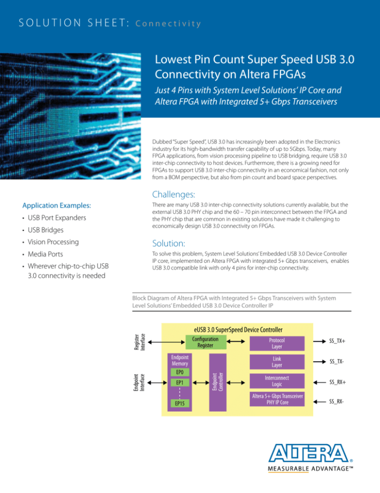
To solve this problem, System Level Solutions’ Embedded USB 3.0 Device Controller
IP core, implemented on Altera FPGA with integrated 5+ Gbps transceivers, enables
USB 3.0 compatible link with only 4 pins for inter-chip connectivity.
• Wherever chip-to-chip USB
3.0 connectivity is needed
Block Diagram of Altera FPGA with Integrated 5+ Gbps Transceivers with System
Level Solutions’ Embedded USB 3.0 Device Controller IP
Configuration
Register
Endpoint
Memory
EP0
EP1
EP15
Endpoint
Controller
Endpoint
Interface
Register
Interface
eUSB 3.0 SuperSpeed Device Controller
Protocol
Layer
SS_TX+
Link
Layer
SS_TX-
Interconnect
Logic
SS_RX+
Altera 5+ Gbps Transceiver
PHY IP Core
SS_RX-
SOLUTION SHEET
Features:
• USB 3.0 compatible link for embedded applications
• Implementation of PHY Layer (with Altera 5+ Gbps transceiver), Link Layer and Protocol Layer
• Supports CONTROL, BULK and ISO transfer without stream support
• Supports 32-bit PHY Layer data interface between Altera Transceiver PHY IP core and Link Layer
• Configurable Endpoint selection
• Option for USB 2.0 compatible link with external USB 2.0 PHY
Supported Devices and Resource Counts
Device
LE
Memory Bits
Memory Blocks
Arria V GX / GT / GZ / SX SoC / ST SoC
~15k
~300,000
47 x M10K
Cyclone V GT / ST SoC
~15k
~300,000
44 x M10K
Stratix V GX / GS / GT
~16k
~300,000
27 x M20K
Development Kits:
• SLS Embedded USB 3.0 Development Board
Features:
• Altera Cyclone V GT FPGA (5CGTFD5C5U19A7)
• Six B-Type USB 3.0 connectors directly connected to Altera transceiver
• Support for JTAG programming mode
• Expandable through HSMC connector
• Memory Subsystem
– DDR2
– SDRAM
– CFI Flash
• User Interface
– 4x push-buttons
– 3 x LEDs
• SLS Embedded USB 3.0 HSMC Board (for use with Altera Cyclone V GT Development Board)
Features:
• Directly connect to Altera Cyclone V GT developboard to use as a USB 3.0 development platform
ment
• Two B-Type and two Micro AB-Type USB 3.0 connectors
Want to Dig Deeper?
For more information about Altera FPGAs and USB 3.0 inter-chip connectivity solution, contact
your Altera representative, or visit the Embedded USB 3.0 Device Controller IP solution page:
http://www.altera.com/eusb3
Altera Corporation
Altera European Headquarters
Altera Japan Ltd.
Altera International Ltd.
101 Innovation Drive
San Jose, CA 95134
USA
www.altera.com
Holmers Farm Way
High Wycombe
Buckinghamshire
HP12 4XF
United Kingdom
Telephone: (44) 1494 602000
Shinjuku i-Land Tower 32F
6-5-1, Nishi-Shinjuku
Shinjuku-ku, Tokyo 163-1332
Japan
Telephone: (81) 3 3340 9480
www.altera.co.jp
Unit 11-18, 9/F
Millennium City 1, Tower 1
388 Kwun Tong Road
Kwun Tong
Kowloon, Hong Kong
Telephone: (852) 2945 7000
©2014 Altera Corporation. All rights reserved. ALTERA, ARRIA, CYCLONE, ENPIRION, MAX, MEGACORE, NIOS, QUARTUS and STRATIX words and logos are trademarks of Altera Corporation and
registered in the U.S. Patent and Trademark Office and in other countries. All other words and logos identified as trademarks or service marks are the property of their respective holders as described at
www.altera.com/legal. September 2014
GEN-1018-1.0
