COPYRIGHT AND TECHNICAL SUPPORT
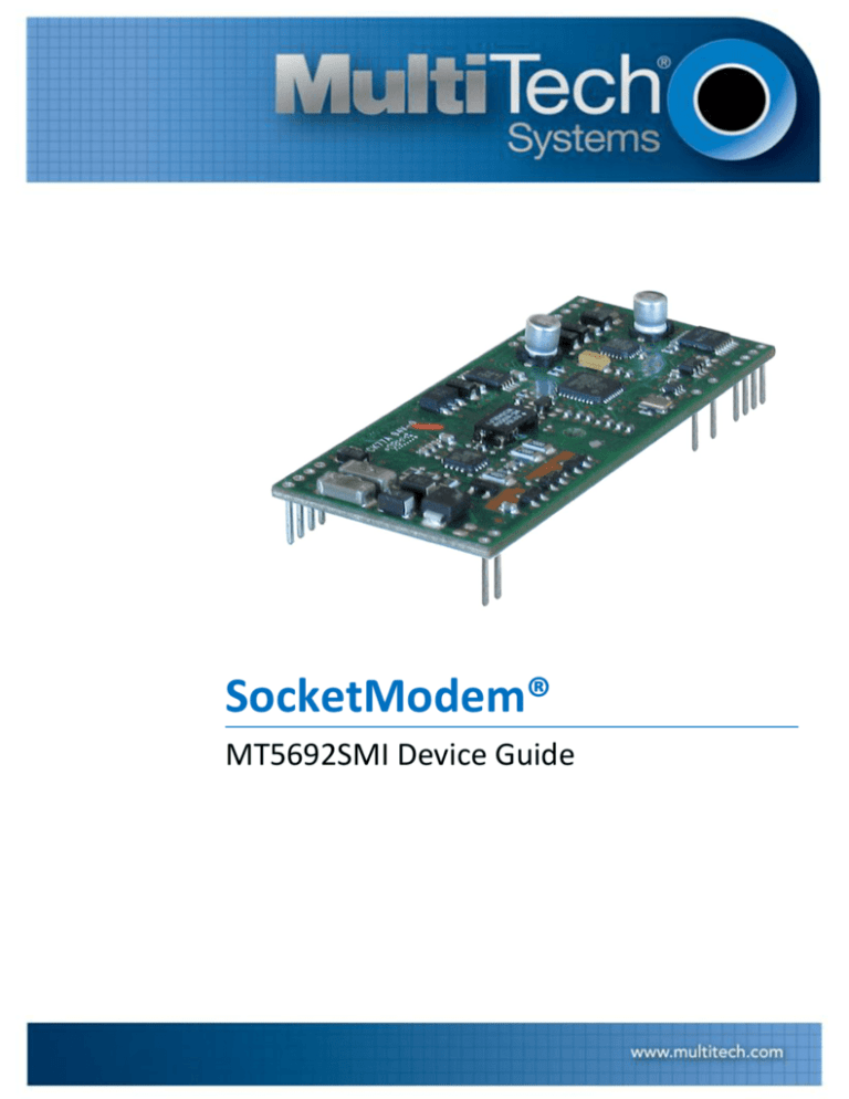
SocketModem®
MT5692SMI Device Guide
Multi-Tech Systems, Inc. Device Guide
1
LEGAL NOTICE AND CONTACT INFORMATION
SocketModem Device Guide
S000535, Version A
MT5692SMI-34, MT5692SMI-L-34, MT5692SMI-92, MT5692SMI-L-92, MT5692SMI-X-L-92, MT5692SMI-IP-92, MT5692SMI-IP-L-92, MT5692SMI-V-34,
MT5692SMI-V-92, MT5692SMI-P-34, MT5692SMI-P-L-34,MT5692SMI-P-92, MT5692SMI-P-L-92
Copyright
This publication may not be reproduced, in whole or in part, without the specific and express prior written permission signed by an executive officer of MultiTech Systems, Inc. All rights reserved. Copyright © 2012 by Multi-Tech Systems, Inc.
Multi-Tech Systems, Inc. makes no representations or warranties, whether express, implied or by estoppels, with respect to the content, information, material
and recommendations herein and specifically disclaims any implied warranties of merchantability, fitness for any particular purpose and non-infringement.
Multi-Tech Systems, Inc. reserves the right to revise this publication and to make changes from time to time in the content hereof without obligation of MultiTech Systems, Inc. to notify any person or organization of such revisions or changes.
Trademarks
Multi Tech, SocketModem, SocketWireless, Universal IP, SocketEthernet IP and the Multi-Tech logo are registered trademarks of Multi-Tech Systems, Inc. All
other brand and product names are trademarks or registered trademarks of their respective companies.
Legal Notices
The Multi-Tech products are not designed, manufactured or intended for use, and should not be used, or sold or re-sold for use, in connection with applications
requiring fail-safe performance or in applications where the failure of the products would reasonably be expected to result in personal injury or death,
significant property damage, or serious physical or environmental damage. Examples of such use include life support machines or other life preserving medical
devices or systems, air traffic control or aircraft navigation or communications systems, control equipment for nuclear facilities, or missile, nuclear, biological or
chemical weapons or other military applications (“Restricted Applications”). Use of the products in such Restricted Applications is at the user’s sole risk and
liability.
The Multi-Tech products and the final application of the Multi-Tech products should be thoroughly tested to ensure the functionality of the Multi-Tech products
as used in the final application. The designer, manufacturer and reseller has the sole responsibility of ensuring that any end user product into which the MultiTech product is integrated operates as intended and meets its requirements or the requirements of its direct or indirect customers. Multi-Tech has no
responsibility whatsoever for the integration, configuration, testing, validation, verification, installation, upgrade, support or maintenance of such end user
product, or for any liabilities, damages, costs or expenses associated therewith, except to the extent agreed upon in a signed written document. To the extent
Multi-Tech provides any comments or suggested changes related to the application of its products, such comments or suggested changes is performed only as a
courtesy and without any representation or warranty whatsoever.
Revisions
Revision
Date
Description
A
12/05/12
Initial release. Information was in the Universal Socket Developer Guide.
Contacting Multi-Tech
Knowledge Base
The Knowledge Base provides immediate access to support information and resolutions for all Multi-Tech products. Visit http://www.multitech.com/kb.go.
Support Portal
To create an account and submit a support case directly to our technical support team, visit: https://support.multitech.com.
Support
Business Hours: M-F, 9am to 5pm CT
Country
By Email
By Phone
Europe, Middle East, Africa:
support@multitech.co.uk
+(44) 118 959 7774
U.S., Canada, all others:
support@multitech.com
(800) 972-2439 or (763) 717-5863
World Headquarters
Multi-Tech Systems, Inc.
2205 Woodale Drive
Mounds View, Minnesota 55112
Phone: 763-785-3500 or 800-328-9717
Fax: 763-785-9874
Warranty
To read the warranty statement for your product, please visit: http://www.multitech.com/warranty.go.
SocketModem MT5692SMI Device Guide
2
CONTENTS
Contents
Chapter 1 – Device Overview ......................................................................................................................................5
Description .......................................................................................................................................................................... 5
Product Build Options ......................................................................................................................................................... 5
Documentation ................................................................................................................................................................... 6
Chapter 2 – Mechanical Drawings ...............................................................................................................................7
Mechanical Drawings – MT5692SMI-34/92 Builds ............................................................................................................. 7
Mechanical Drawings – MT5692SMI-X-L-92 no LEDs 3.3V Build ........................................................................................ 8
Mechanical Drawings – MT5692SMI-V Voice Builds........................................................................................................... 9
Mechanical Drawings – Parallel Builds.............................................................................................................................. 10
Chapter 3 – Specifications ........................................................................................................................................ 11
Technical Specifications .................................................................................................................................................... 11
Mounting Hardware .......................................................................................................................................................... 12
Device Reset ...................................................................................................................................................................... 13
Reset Line Interface ........................................................................................................................................................................ 13
Operating Conditions ........................................................................................................................................................ 13
DC Electrical Characteristics .............................................................................................................................................. 13
Absolute Maximum Rating .............................................................................................................................................................. 14
Pin Descriptions for a Parallel SocketModem ................................................................................................................... 14
Power Measurements ....................................................................................................................................................... 15
Chapter 4 – Application Notes .................................................................................................................................. 17
Tip and Ring Interface ....................................................................................................................................................... 17
Recommended Uses for Filtering Options ...................................................................................................................................... 17
Microphone and Speaker .................................................................................................................................................. 18
Microphone Input Option ............................................................................................................................................................... 18
Speaker Output Option 1 ................................................................................................................................................................ 18
Speaker Output Option 2 ................................................................................................................................................................ 18
Speaker Output ............................................................................................................................................................................... 19
Chapter 5 – Parallel Devices ..................................................................................................................................... 20
Parallel Host Bus Timing.................................................................................................................................................... 20
Timing Requirements for Parallel Write ......................................................................................................................................... 20
Timing Requirements for Parallel Read .......................................................................................................................................... 20
SocketModem Parallel Interface....................................................................................................................................... 21
FIFO Mode Selected ........................................................................................................................................................................ 21
FIFO Mode Not Selected ................................................................................................................................................................. 21
Receive Data ................................................................................................................................................................................... 21
3
SocketModem MT5692SMI Device Guide
CONTENTS
Transmit Data .................................................................................................................................................................................. 21
Receiver FIFO interrupt operation .................................................................................................................................................. 22
Transmitter FIFO Interrupt Operation ............................................................................................................................................ 22
Register Functional Definitions ......................................................................................................................................... 23
Internal Registers ............................................................................................................................................................................ 23
IER – Interrupt Enable Register ....................................................................................................................................................... 24
FCR – FIFO Control Register ............................................................................................................................................................ 25
IIR – Interrupt Identifier Register .................................................................................................................................................... 25
LCR – Line Control Register ............................................................................................................................................................. 27
MCR – Modem Control Register ..................................................................................................................................................... 28
LSR – Line Status Register ............................................................................................................................................................... 28
MSR – Modem Status Register........................................................................................................................................................ 29
RBX – RX Buffer (Receiver Buffer Register) ..................................................................................................................................... 30
THR – TX Buffer (Transmitter Holding Register).............................................................................................................................. 30
SCR – Scratch Register..................................................................................................................................................................... 30
Divisor Registers .............................................................................................................................................................................. 30
SocketModem MT5692SMI Device Guide
4
CHAPTER 1 – DEVICE OVERVIEW
Chapter 1 – Device Overview
Description
The Multi-Tech SocketModem creates communication-ready devices by integrating data, fax, and voice
functionality into a single product design. The SocketModem is a space-efficient, embedded modem that provides
V.92 or V.34/33.6K data communication.
The MT5692SMI SocketModem:
Is a standard 64-pin modem used for integrating data communications.
Is a single-port modem that integrates the controller, DSP, and DAA in a 1" x 2.5" form factor and communicates
to a host controller via an asynchronous serial interface.
Is available with an 8-bit parallel interface.
The SocketModem IP, MT5692SMI-IP, embedded modem creates Internet-ready devices by integrating modem
functionality and a complete TCP/IP protocol stack into a single, universal socket design. This embedded modem
sends and receives data via e-mail, HTTP, or socket interfaces. It also complies with global telecom requirements
allowing for worldwide shipments.
This device guide covers the SocketModem MT5692SMI and its various builds: serial, parallel, voice. The serial
build option can be ordered with or without IP functionality.
Product Build Options
Product
Serial Builds
MT5692SMI-34
MT5692SMI-L-34
MT5692SMI-92
MT5692SMI-L-92
MT5692SMI-X-L-92
IP Builds
MT5692SMI-IP-92
MT5692SMI-IP-L-92
Voice Builds
MT5692SMI-V-34
MT5692SMI-V-92
Parallel Builds
MT5692SMI-P-34
MT5692SMI-P-L-34
MT5692SMI-P-92
MT5692SMI-P-L-92
Developer Kit
MTSMI-UDK
MTSMI-P-UDK
5
Description
Region
V.34 Serial Data / V.17 Fax, 5V
V.34 Serial Data / V.17 Fax, 3.3V
V.92 Serial Data / V.17 Fax, 5V
V.92 Serial Data / V.17 Fax, 3.3V
V.92 Serial Data / V.17 Fax, 3.3V (excludes LED pins)
Global
Global
Global
Global
Global
V.92 Serial Data-Only, 5V, Universal IP
V.92 Serial Data-Only, 3.3V, Universal IP
Global
Global
V.34 Serial Data / V.17 Fax / Voice, 5V
V.92 Serial Data / V.17 Fax / Voice, 5V
Global
Global
V.34 Parallel Data / V.17 Fax, 5V
V.34 Parallel Data / V.17 Fax, 3.3V
V.92 Parallel Data / V.17 Fax, 5V
V.92 Parallel Data / V.17 Fax, 3.3V
Global
Global
Global
Global
Universal Developer Kit
SocketModem Parallel Developer Kit
Global
Global
SocketModem MT5692SMI Device Guide
CHAPTER 1 – DEVICE OVERVIEW
Notes:
Voice builds include microphone and speaker pins.
All builds can be ordered individually or in 50-packs.
The complete product code may end in .Rx, for example MT5692SMI.Rx, where R is revision and x is the
revision number.
Documentation
The following documentation is available by email to oemsales@multitech.com or by using the Developer Guide
Request Form on the multitech.com website.
Device Guides – This document. Provides model-specific specifications and developer information.
Universal Socket Developer Guide – Provides an overview, safety and regulatory information, design
considerations, schematics, and general device information.
AT Command Guide – Use the following AT Command Guides:
S000468 for MT5692SMI Modems
S000457 Universal IP Commands
SocketModem MT5692SMI Device Guide
6
CHAPTER 2 – MECHANICAL DRAWINGS
Chapter 2 – Mechanical Drawings
MT5692SMI-34/92 Builds
7
SocketModem MT5692SMI Device Guide
CHAPTER 2 – MECHANICAL DRAWINGS
MT5692SMI-X-L-92 no LEDs 3.3V Build
SocketModem MT5692SMI Device Guide
8
CHAPTER 2 – MECHANICAL DRAWINGS
MT5692SMI-V Voice Builds
9
SocketModem MT5692SMI Device Guide
CHAPTER 2 – MECHANICAL DRAWINGS
Parallel Builds
SocketModem MT5692SMI Device Guide
10
CHAPTER 3 –SPECIFICATIONS
Chapter 3 – Specifications
Technical Specifications
Category
General
Standards
Description
V.92, V.34, V.32bis, V.32, V.23, V.23 half-duplex, V.23 reverse, V.22bis, V.22bis Fast
Connect, V.22, V.21, Bell 212A/Bell 103, V.29 FastPOS, V.80 Synchronous Access Mode
(V.80 not for IP build)
Speed, Format, Compression
Serial/Data Speeds
All builds except IP: Supports DTE speeds up to 230.4Kbps, autobaud up to 115.2Kbps
For IP build: Supports DTE speeds up to 921.6Kbps
Client-to-Client Data Rates 33600, 31200, 28800, 26400, 24000, 21600, 19200, 16800, 14400, 12000, 9600, 7200,
4800, 2400, 1200, 0-300 bps
Data Format
All builds: Serial, asynchronous
Parallel build: 8-bit parallel interface
Character Format
10-bit
Data Error Correction
V.42 LAPM and MNP 2–4
(ECM)
Data Compression
V.44, V.42bis, MNP 5
Fax
Fax Compatibility
All builds except IP: V.17, V.29, V.27ter, V.21 channel 2
Fax Class
All builds except IP: Class 1 &1.0
Operation Modes
Full duplex over dial-up lines; data mode; command mode; online command mode
Physical Description
Weight
0.6 oz. (0.017kg)
Dimensions
2.541” L x 1.045” W x 0.44” H (6.45cm L x 2.65cm W x 1.1 cm H)
Voice build: 2.541” L x 1.045” W x 0.535” H (6.45cm L x 2.65cm W x 1.4cm H)
Consult mechanical drawings for model specific variance.
Environment
Operating Temperature
-40° C to +85° C
Storage Temperature
-40° C to +85° C
Humidity
20% to 90% non-condensing
Power Requirements
Operating Voltage
3.3V or 5V depending on build; voice models are 5V only
11
SocketModem MT5692SMI Device Guide
CHAPTER 3 – SPECIFICATIONS
Category
Transmission
Transmit Level
Receiver Sensitivity
DAA Isolation
Flow Control
Command Buffer
Telephony/TAM
Description
- 12 dBm (varies by country setting)
- 43 dBm under worst-case conditions
1.5Kv r.m.s. or 2121 VDC at working voltage of 250VAC
All builds except IP: XON/XOFF (software), RTS/CTS (hardware)
60 characters
All builds except voice:
V.253 commands
8 kHz sample rate
Concurrent DTMF, distinctive ring, and "Bell Core Type 1" Caller ID
8-bit μ-law and A-law PCM coding
Supports PCM encoding: 8-bit and 16-bit linear PCM; and 4-bit IMA coding
Voice build: Voice build has a microphone for speakerphone function
IP, M2M, SMS
Supported IP Protocols
For IP build only:
Internet Protocols Supported: Dial-in PPP, DNS, FTP, ICMP,IP, LCP, PPP, SMTP,
SNTP, TCP, UDP Socket
Authentication Protocols: CHAP, Dial-up Script, PAP
Certifications, Compliance, Warranty
EMC Compliance
FCC Part 15 (Class B)
ICES-003 (Class B)
EN 55022 (Class B)
EN 55024
Safety Compliance
UL 60950-1
cUL 60950-1
EN 60950-1
AS/NZS 60950:2003
Telecom Compliance
47 CFR Part 68
CS-03
R&TTE
A-Tick (Other countries included per the Modem Globalization Guide)
Warranty
Two years
Mounting Hardware
#2 or M2 for hardware should be used for mounting the analog modem on the board when the tooling hole
diameter on the board is .093.
#4 or M3 for hardware should be used for mounting the analog modem on the board when the tooling hole
diameter on the board is .128
Important:
There are traces and vias around the tooling holes, so use nylon hardware if you are using the tooling holes
to mount the SocketModems on the board.
SocketModem MT5692SMI Device Guide
12
CHAPTER 3 –SPECIFICATIONS
Device Reset
The SocketModem is ready to accept commands after a fixed amount of time (“X” Time) after power-on or reset.
Model
Time Constant
"X" Time
MT5692SMI
250 ms
6 seconds
1
The SocketModem may respond to a shorter reset pulse.
Minimum Reset Pulse1
100us
Reset Line Interface
The modem’s reset line employs a 10K pull up resistor. If using an open collector driver, run that output to the
modem only and use a separate driver for other embedded components. The modem’s reset signal may also be
driven by a circuit that both sinks and sources current. These modems do not require an external reset. They have
their own internal reset circuitry and voltage monitor and will function correctly even if the reset input is open.
Modem Reset (with weak pull-up)
The active low –RESET input resets the SocketModem logic and returns the AT command set to the original factory
default values or to "stored values" in NVRAM. The modem is ready to accept commands within 6 seconds of
power-on or reset. Reset must be asserted for a minimum of 100 ns.
Operating Conditions
Parameter
5V Supply Range – Vcc
3.3V Supply Range – Vcc
Minimum
4.5V
3.135V
Maximum
5.5V
3.465V
DC Electrical Characteristics
Units: Volts
5VDC Characteristics (VDD = 5V ± 0.25V) VDDMAX = 5.25V
3.3VDC Characteristics (VDD = 3.3V ± 0.3V) VDDMAX = 3.6V
Parameter
5V Serial SocketModem
Digital Inputs
–DTR (40), –TXD (35), –RTS (33), –Reset (24)
Digital Outputs
–DCD (39), –CTS (38), –DSR (37), –RI (36), –RXD (34)
Digital Input Capacitance
5V Parallel SocketModem
Digital Inputs
A0 (31), A1 (25), –WR (32), –RD (33), –DS (40)
Digital Outputs
DO (37), D1 (38), D2 (29), D3 (39), D4 (35), D5 (36), D6 (41), D7 (27), INT (30)
Digital Input Capacitance
13
Minimum
Maximum
Input High
Min 2.2V
Output High
Min 2.9V
Input Low
Max .8V
Output Low
Max 0.4V
50 pF
Input High
Min 2.2V
Output High
Min 2.4V
Input Low
Max 0.8V
Output Low
Max 0.4V
50pF
SocketModem MT5692SMI Device Guide
CHAPTER 3 – SPECIFICATIONS
3.3V Serial SocketModem
Digital Inputs
–DTR (40), –TXD (35), –RTS (33), –Reset (24)
Digital Outputs
–DCD (39), –CTS (38), –DSR (37), –RI (36), –RXD (34)
Digital Input Capacitance
3.3V Parallel SocketModem
Digital Inputs
A0 (31), A1 (25), A2 (34), –WR (32), –RD (33), –DS (40)
Digital Outputs
DO (37), D1 (38), D2 (29), D3 (39), D4 (35), D5 (36), D6 (41), D7 (27), INT (30)
Digital Input Capacitance
Input High
Min 2.2V
Output High
Min. 2.9V
Input Low
Max 0.8V
Output Low
Max 0.4V
50 pF
Input High
Min 2V
Output High
Min 2V
Input Low
Max 0.8V
Output Low
Max 0.4V
50 pF
Absolute Maximum Rating
Voltage at any signal pin: GND -0.3V Maximum VCC +3.3V
Pin Descriptions for a Parallel SocketModem
Note: Consult the Universal Socket Developer Guide for serial SocketModem pin information.
Pin # Signal
1
Tip
I/O
I/O
2
Ring
I/O
24
–RESET I
25
A1
I
26
27
29
30
DGND
D7
D2
INT
GND
O
O
O
31
A0
I
32
–WR
I
Description
Tip Signal from Telco. Tip connection to the phone line (RJ-11 Pin 4). The SocketModem is
Tip/Ring polarity insensitive.
Ring Signal from Telco. Ring connection to the phone line (RJ-11 Pin 3). The SocketModem
is Tip/Ring polarity insensitive.
Device Reset (with pull-up). The active low –RESET input resets the device logic and
returns the configuration of the device to the original factory default values or "stored
values" in the NVRAM.
–RESET is tied to VCC through a time-constant circuit for “Power-on-Reset” functionality.
The SocketModem is ready to accept commands after a fixed amount of time (“X” Time)
after power-on or reset.
Refer to Device Reset for more information.
Host Bus Address Line 0. During a host read or write operation, A0 selects an internal
16C450 or 16C550-compatible register. The state of the divisor latch access bit (DLAB)
affects the selection of certain registers.
Digital Ground
Data Bus. See pin 35.
Data Bus. See pin 35.
Host Bus Interrupt. INT output is set high when the receiver error flag, receiver data
available, transmitter holding register empty, or modem status interrupt have an active
high condition. INT is reset low upon the appropriate interrupt service or master reset
operation.
Host Bus Address Line 1. During a host read or write operation, A1 selects an internal
16C450 or 16C550-compatible register. The state of the divisor latch access bit (DLAB)
affects the selection of certain registers.
Host Bus Write. –WR is an active low, write control input. When –DS is low, –WR low
allows the host to write data or control words into a selected modem register.
SocketModem MT5692SMI Device Guide
14
CHAPTER 3 –SPECIFICATIONS
Pin # Signal
33
–RD
I/O
I
34
A2
I
35
36
37
38
39
40
41
61
63
D4
D5
D0
D1
D3
–DS
D6
VCC
AGND
I
O
O
O
O
I
O
PWR
GND
64
SPKR
O
Description
Host Bus Read. –RD is an active low, read control input. When –DS is low, –RD low allows
the host to read status information or data from a selected modem register.
Host Bus Address Line 2. During a host read or write operation, A2 selects an internal
16C450 or 16C550-compatible register. The state of the divisor latch access bit (DLAB)
affects the selection of certain registers.
Data Bus. These pins are the eight bit, tristate data bus for transferring information to or
from the controlling CPU. D0 is the least significant bit and the first
data bit in a transmit or receive serial data stream.
Host Bus Device Select. –DS input low enables the modem for read or write.
Data Bus. See pin 35.
+5V or 3.3V Supply (depends upon model).
Analog Ground. This is tied common with DGND on the SocketModem. To minimize
potential ground noise issues, connect audio circuit return to AGND.
Speaker. Dual purpose output for call progress signals or speakerphone functions.
Call Progress signaling on MT5692SMI is a square wave output that can be optionally
connected to a low-cost single-ended speaker; e.g., a sounducer or an analog speaker
circuit.
Speakerphone Output on the MT5692SMI is under the control of +FCLASS. This is a singleended analog output. SPKR is tied directly to the CODEC. One side of a differential AC
output coupled through a 6.8K ohm resistor and capacitor.
Power Measurements
Multi-Tech Systems, Inc. recommends that you incorporate a 10% buffer into your power source when
determining product load.
Sleep Mode Typical
MT5692SMI-Serial Build at 3.3 Volts
Current (AMPS)
0.014
0.069
Watts
0.046
0.216
MT5692SMI-Serial Build at 5.0 Volt
Current (AMPS)
0.018
0.074
Watts
0.089
0.359
MT5692SMI-IP Build at 3.3 Volt
Current (AMPS)
0.047
0.101
Watts
0.151
0.316
MT5692SMI-IP Build at 5.0 Volt
Current (AMPS)
0.052
0.109
Watts
0.256
0.528
MT5692SMI-V Build at 5.0 Volt (Voice build)
Current (AMPS)
0.016
0.076
Watts
0.080
0.380
15
Maximum1
0.080
0.249
0.088
0.425
0.112
0.349
0.121
0.583
0.089
0.445
SocketModem MT5692SMI Device Guide
CHAPTER 3 – SPECIFICATIONS
MT5692SMI-P Build at 3.3 Volt (Parallel build)
Measured voltage
3.30
3.29
3.29
Current (AMPS)
0.015
0.072
0.081
Watts
0.051
0.236
0.267
MT5692SMI-P Build at 5.0 Volt (Parallel build)
Measured voltage
4.91
4.86
4.84
Current (AMPS)
0.014
0.069
0.079
Watts
0.068
0.334
0.380
1
Maximum: The continuous current during maximum data rate at maximum power.
Notes:
Voice builds are not available in 3.3V builds.
SocketModem MT5692SMI Device Guide
16
CHAPTER 4 –APPLICATION NOTES
Chapter 4 – Application Notes
Tip and Ring Interface
OEM Motherboard Filtering and Surge Protection Options
See Design Considerations and Recommended Parts in the Universal SocketModem Developer Guide.
Recommended Uses for Filtering Options
17
Enhanced Surge Protection with RJ-11 Filtering
Use this option when additional lightning protection may be needed.
Alternate Common Mode with RJ-11 Filtering
Use this option when your design has common mode emission issues.
SocketModem MT5692SMI Device Guide
CHAPTER 4 –APPLICATION NOTES
Microphone and Speaker
Note: Applies to the MT5692SMI Voice only.
Microphone Input Option
Speaker Output Option 1
Speaker Output Option 2
Differences between Options 1 and 2: Speaker 1 does not have an amplifier while Speaker 2 does.
SocketModem MT5692SMI Device Guide
18
CHAPTER 4 –APPLICATION NOTES
Specifications for the Microphone Input
Impedance
AC Input Voltage Range
Reference Voltage
>70K
1.1V P-P
1.35V
Specifications for the Speaker Output from the Codec
Minimum Load
Maximum Capacitive Load
Output Impedance
AC Output Voltage Range
Reference Voltage
DC Offset Voltage
300
0.01 uF
10
1.4V P-P
+1.35 VDC
20 mV
Speaker Output
The speaker output from the codec is coupled to the speaker pin (64) through a 1uF cap and a 33 ohm resistor.
The speaker pin is shared with the call progress monitor which is a digital I/O pin on the DSP that is coupled to the
speaker pin through a 1uF and 3.9K.
19
SocketModem MT5692SMI Device Guide
CHAPTER 5 – PARALLEL DEVICES
Chapter 5 – Parallel Devices
Parallel Host Bus Timing
Timing Requirements for Parallel Write
Symbol
t
AS
t
AH
t
CS
t
CH
t
WT
t
DS
t
DWH
Parameter
Address Setup
Address Hold
Chip Select Setup
Chip Select Hold
WT Strobe Width
Write Data Setup
Write Data Hold
Min
5
5
0
10
15
15
5
Max
20
-
Unit
Ns
Ns
Ns
Ns
Ns
Ns
Ns
Min
5
5
5
0
77
10
5
Max
25
-
Unit
Ns
Ns
Ns
Ns
Ns
Ns
Ns
Timing Requirements for Parallel Read
Symbol
t
AS
t
AH
t
CS
t
CH
t
RD
t
DD
t
DRH
Parameter
Address Setup
Address Hold
Chip Select Setup
Chip Select Hold
RD Strobe Width
Read Data Delay
Read Data Hold
Notes:
When the host executes consecutive Rx FIFO reads, a minimum delay of 2 times the internal CPU clock cycle
plus 15 ns (85.86 ns at 28.224 MHz) is required from the falling edge of RD to the falling edge of the next
Host Rx FIFO RD clock.
When the host executes consecutive Tx FIFO writes, a minimum delay of 2 times the internal CPU clock cycle
plus 15 ns (85.86 ns at 28.224 MHz) is required from the falling edge of WT to the falling edge of the next
Host Tx FIFO WT clock.
t
RD' tWT = tCYC + 15 ns.
t
DS is measured from the point at which both CS and WT are active.
t
DWH is measured from the point at which either CS and WT become active.
Clock Frequency = 1.8432 MHz clock.
SocketModem MT5692SMI Device Guide
20
CHAPTER 5 – PARALLEL DEVICES
Parallel host bus – read
Parallel host bus - write
SocketModem Parallel Interface
The modem supports a 16550A interface in parallel interface versions. The 16550A interface can operate in FIFO
mode or non-FIFO mode. Non-FIFO mode is the same as the 16450-interface operation.
The modem emulates the 16450/16550A interface and includes both a 16-byte receiver data first-in first-out
buffer (RX FIFO) and a 16-byte transmit data first-in first-out buffer (TX FIFO).
FIFO Mode Selected
When FIFO mode is selected in the FIFO Control Register (FCR0 = 1), both FIFOs are operative.
FIFO Mode Not Selected
When FIFO mode is not selected, operation is restricted to a 16450-interface operation.
Receive Data
The host reads received data from the Receiver Buffer (RX Buffer). The RX Buffer corresponds to the Receiver
Buffer Register in a 16550A device. In FIFO mode, the RX FIFO operates transparently behind the RX Buffer.
Interface operation is described with reference to the RX Buffer in FIFO and non-FIFO modes.
Transmit Data
The host loads transmit data into the Transmit Buffer (TX Buffer). The TX Buffer corresponds to the Transmit
Holding Register in a 16550A device. In FIFO mode, the TX FIFO operates transparently behind the TX Buffer.
Interface operation is described with reference to the TX Buffer in both FIFO and non-FIFO modes.
21
SocketModem MT5692SMI Device Guide
CHAPTER 5 – PARALLEL DEVICES
Receiver FIFO interrupt operation
Receiver Data Available Interrupt
When you enable FIFO mode (FCR0 = 1) and receiver interrupt (RX Data Available) (IER0 = 1), the receiver interrupt
operates as follows:
1. The Receiver Data Available Flag (LSR0) is set as soon as a received data character is available in the RX FIFO.
LSR0 clears when RX FIFO is empty.
2. The Receiver Data Available interrupt code (IIR0-IIR4 = 4h) is set whenever the number of received data bytes
in the RX FIFO reaches the trigger level specified by FCR6-FCR7 bits. It clears whenever the number of received
data bytes in the RX FIFO drops below the trigger level specified by FCR6-FCR7 bits.
3. The HINT interrupt is asserted whenever the number of received data bytes in the RX FIFO reaches the trigger
level specified by FCR6-FCR7 bits. HINT interrupt is de-asserted when the number of received data bytes in the
RX FIFO drops below the trigger level specified by FCR6-FCR7 bits.
Receiver Character Timeout Interrupts
When you enable the FIFO mode (FCR0 = 1) and receiver interrupt (Receiver Data Available) (IER0 = 1), the
receiver character timeout interrupt operates as follows:
A Receiver Character Timeout interrupt code (IIR0-IIR3 = Ch) is set if at least one received character is in the RX
FIFO, the most recent received serial character is longer than four continuous character times ago (if 2 stop bits
are specified, the second stop bit is included in this time period), and the most recent RX FIFO host read is longer
than four continuous character times ago.
Transmitter FIFO Interrupt Operation
Transmitter Empty Interrupt
When you enable FIFO mode (FCR0 = 1) and transmitter interrupt (TX Buffer Empty) (IER0 =1), the transmitter
interrupt operates as follows:
1. The TX Buffer Empty interrupt code (IIR0-IIR3 = 2h) occurs when the TX Buffer is empty. It clears when the TX
Buffer is written to (1 to 16 characters) or the IIR is read.
2. The TX Buffer Empty indications will be delayed 1 character time minus the last stop bit time whenever the
following occur:
THRE = 1 and there has not been at least two bytes at the same time in the TX FIFO Buffer since the last
setting of THRE was set. The first transmitter interrupt after setting FCR0 will be immediate.
SocketModem MT5692SMI Device Guide
22
CHAPTER 5 – PARALLEL DEVICES
Register Functional Definitions
The following table and descriptions define the assigned bit functions for the twelve internal registers.
Internal Registers
Reg.
No.
7
6
5
Register
Name
Scratch
Register
(SCR)
Modem
Status
Register
(MSR)
BIT-7
BIT-6
BIT-5
BIT-3
BIT-2
BIT-1
BIT-0
Delta Data
Set Ready
(DDSR)
Delta
Clear to
Send
(DCTS)
Break
Framing
Interrupt Error
(BI)
(FE)
Trailing
Edge of
Ring
Indicator
(TERI)
Parity
Error
(PE)
Overrun
Error (OE)
Receiver
Data
Ready
(DR)
0
Out 2
Out 1
Even
Parity
Select
(EPS)
Parity
Enable
(PEN)
0
Pending
Pending
Interrupt ID Interrupt
Bit 2
ID
Bit 1
Scratch Register
Data
Carrier
Detect
(DCD)
Ring
Indicator
(RI)
Data Set
Clear to Delta Data
Ready (DSR) Send
Carrier
CTS)
Detect
(DDCD)
Line Status RX FIFO Transmitter Transmitter
Register
Error
Empty
Buffer
(LSR)
(TEMT)
Register
Empty
(THRE)
4
Modem
0
0
0
Control
Register
(MCR)
3
Line Control Divisor Set Break Stick Parity
Register
Latch
(LCR)
Access
Bit
(DLAB)
2
Interrupt
FIFOs
FIFOs
0
Identify
Enabled Enabled
Register
(IIR)
(Read Only)
2
FIFO
Receiver Receiver
Reserved
Control
Trigger Trigger
Register
MSB
LSB
(FCR)
(Write Only)
1
Interrupt
0
0
0
(DLAB Enable
= 0)
Register
(IER)
23
BIT-4
Request to Data
Send (RTS) Terminal
Ready
(DTR)
Number of Word
Word
Stop Bits Length
Length
(STB)
Select Bit 1 Select Bit
(WLS1)
0 (WLSO)
Pending
“0” if
Interrupt ID Interrupt
Bit 0
Pending
Reserved 0
TX FIFO
Reset
RX FIFO
Reset
FIFO
Enable
0
Enable
Receiver
Line Status
Interrupt
(ELSI)
Enable
Transmitter
Holding
Register
Empty
Interrupt
(ETBEI)
Enable
Received
Data
Available
Interrupt
(ERBFI)
Enable
Modem
Status
Interrupt
(EDSSI)
SocketModem MT5692SMI Device Guide
CHAPTER 5 – PARALLEL DEVICES
Reg.
No.
0
(DLAB
= 0)
Register
Name
Transmitter
Buffer
Register
(THR)
0
Receiver
(DLAB Buffer
= 0)
Register
(RBR)
1
Divisor
(DLAB Latch MSB
= 1)
Register
(DLM)
0
Divisor
(DLAB Latch LSB
= 1)
Register
(DLL)
BIT-7
BIT-6
BIT-5
BIT-4
BIT-3
BIT-2
BIT-1
BIT-0
Transmitter FIFO Buffer Register (Write Only)
Receiver FIFO Buffer Register (Read Only)
Divisor Latch MSB
Divisor Latch LSB
IER – Interrupt Enable Register
(Addr = 1, DLAB = 0)
The IER enables five interrupt types that can separately assert the HINT output signal (Refer to Interrupt Sources
and Reset Control in the IIR).
To enable a selected interrupt:
Set the corresponding enable bit to 1.
To disable a selected interrupt:
Set the corresponding enable bit to 0.
Disabling an interrupt in the IER keeps you from setting the corresponding indication in the IIR and HINT assertion.
Disabling all interrupts (resetting IER0 – IER3 to a 0) prevents setting any Interrupt Identifier Register (IIR) bits and
HINT output assertion. All other system functions operate normally.
Bit
7-4
3
Description
Not used.
Enable Modem Status
Interrupt (EDSSI)
2
Enable Receiver Line Status
Interrupt (ELSI)
SocketModem MT5692SMI Device Guide
Settings
Always 0.
1 enables HINT output assertion whenever the Delta CTS (MSR0), Delta
DSR (MSR1), Delta TER (MSR2), or Delta DCD (MSR3) bit in the Modem
Status Register (MSR) is 1.
0 disables HINT assertion due to the any of the four MSR bit settings.
1 enables HINT output assertion when the Overrun Error (LSR1), Parity
Error (LSR2), Framing Error (LSR3), or Break Interrupt (LSR4) receiver status
bit in the Line Status Register (LSR) changes state.
0 disables HINT assertion due to LSR5.
24
CHAPTER 5 – PARALLEL DEVICES
Bit
1
Description
Enable Transmitter Holding
Register Empty Interrupt
(ETBEI)
Enable Receiver Data
Available Interrupt (ERBFI)
and Character Timeout in
FIFO Mode
0
Settings
1 enables HINT output assertion when the Transmitter Empty bit in the
Line Status Register (LSR5) is 1.
0 disables assertion of HINT due to LSR5.
1 enables HINT output assertion when the Receiver Data Ready bit in the
Line Status Register (LSR0) is 1 or character timeout occurs in the FIFO
mode.
0 disables HINT assertion due to the LSR0 or character timeout.
FCR – FIFO Control Register
(Addr = 2, Write Only)
FCR is a write-only register used to enable FIFO mode, clear the RX FIFO and TX FIFO, enable DMA mode, and set
the RX FIFO trigger level.
Bit Description
7-6 RX FIFO Trigger Level
5-4 Not Used
3 DMA Mode Select – Must be
set to zero.
Settings
FCR7 and FCR6 set the trigger level for the RX FIFO (Receiver Data Available)
interrupt.
7
6
RX FIFO Trigger Level (Bytes)
0
0
01
0
1
04
1
0
08
1
1
14
When FIFO is selected, FCR0= 1, FCR3 selects non-DMA operation (FCR3=0) or
DMA operation (FCR3=1).
When FIFO mode is not selected, FCR0=0, this bit is not used and the modem
operates in non-DMA mode in 16450 operation.
DMA Operation in FIFO Mode Not Supported
Non-DMA Operation in FIFO RXRDY asserted when there are one or more characters in the RX FIFO. It is
Mode
inactive when there are no more characters in the RX FIFO.
2
TX FIFO Reset
1
RX FIFO Reset
0
FIFO Enable
TXRDY asserted when there are no characters in the TX FIFO. It is inactive
when the character is loaded into the TX FIFO Buffer.
When FCR2=1, all bytes in the TX FIFO are cleared. The modem automatically
clears this bit.
When FCR1=1, all bytes in the RX FIFO are cleared, The modem automatically
clears this bit.
When FCR0=0, 16450 mode is selected and all bits are cleared in both FIFOs.
When FCR0=1, FIFO mode (16550A) is selected and both FIFOs are enabled.
FCR0 must be 1 when other bits in the FCR are written or they will not be acted
upon.
IIR – Interrupt Identifier Register
(Addr = 2)
25
SocketModem MT5692SMI Device Guide
CHAPTER 5 – PARALLEL DEVICES
The Interrupt Identifier Register (IIR) identifies the existence and up to five prioritized pending interrupts types.
Set four priority levels to assist interrupt processing in the host. The four levels, in decreasing priority, are highest
receiver line status, receiver data available or receiver character timeout, TX buffer empty, and modem status.
The modem freezes all interrupts and indicates the highest priority interrupt pending when the IIR is accessed.
Until this access is complete, changes occurring in interrupt conditions are not indicated.
Bit
7-6
5-4
3-1
Description
FIFO Mode
Not Used
Highest Priority Pending
Interrupt
0
Interrupt Pending
Settings
These bits copy FCR0.
Always 0.
These bits identify the highest priority pending interrupt. Bit 3 is applicable only
when FIFO mode is selected; otherwise, bit 3 is a 0. Refer to Interrupt Sources
and Reset Control for details.
When this bit is a 0, an interrupt is pending; IIR bits 1-3 can be used to determine
the source of the interrupt. When this bit is a 1, an interrupt is not pending.
Interrupt Sources and Reset Control Table
Interrupt Identification Register
Bit 31 Bit 2 Bit 1 Bit 0 Priority
0
0
0
1
—
0
1
1
0
Highest
0
1
0
0
2
1
1
0
0
2
0
0
1
0
3
Interrupt Set and Reset Functions
Interrupt Type
Interrupt Source
None
None
Receiver Line
Overrun Error (OE) (LSR1),
Status
Parity Error (PE) (LSR2),
Framing Error (FE) (LSR3),
or Break Interrupt (BI)
(LSR4)
Received Data
Received Data Available
Available
(LSR0)
or RX FIFO Trigger Level
(FCR6-FCR7)
Reached1
Character
The RX FIFO contains at
Timeout
least 1 character and no
Indication1
characters have been
removed from or input to
the RX FIFO during the last
4 character times.
TX Buffer Empty TX Buffer Empty
0
0
0
0
4
Modem Status
Delta CTS (DCTS) (MSR0),
Delta DSR (DDST) (MSR1),
Trailing Edge Ring Indicator
(TERI) (MSR3), or Delta
DCD (DCD) (MSR4)
Interrupt Reset Control
—
Reading the LSR
Reading the RX Buffer or
the RX FIFO drops below
the Trigger Level
Reading the RX Buffer
Reading the IIR or writing
to the TX Buffer
Reading the MSR
1
FIFO Mode only.
SocketModem MT5692SMI Device Guide
26
CHAPTER 5 – PARALLEL DEVICES
LCR – Line Control Register
(Addr = 3)
The Line Control Register (LCR) specifies the format of the asynchronous data communications exchange.
Bit
7
Description
Divisor Latch Access Bit
(DLAB)
6
Set Break
5
27
Stick Parity
4
Even Parity Select (EPS)
3
Enable Parity (PEN)
2
Number of Stop GBITS
(STB)
1-0
Word Length Select
(WLS0 and WLS1)
Settings
To access the Divisor Latch Registers during a read or write operation, set to 1.
To access the Receive Buffer, Transmitter Buffer, or Interrupt Enable Register, it
must be reset to a 0.
Bit 6=1 Transmit Data forced to break condition and space (0) is sent.
Bit 6=0, break is not sent. The Set Break bit acts only on Transmit Data and has
no effect on the serial in logic.
When Parity is enabled (LCR3=1) and Stick Parity selected (LCR5=1), the parity is
transmitted and checked by the receiver:
As 0 if even parity is selected (LCR4=1)
As 1 if odd parity is selected (LCR4=0)
When Stick Parity is not selected (LCR3 = 0), parity is transmitted and checked as
determined by the LCR3 and LCR4 bits.
When Parity is enabled (LCR3=1) and Stick Parity not selected (LCR5=0), the
number of 1s transmitted or checked by the receiver in the data word bits and
parity bit is:
Even, LCR4=1
or
Odd, LCR4=0
When Bit 3= 1, a parity bit is generated in the serial out (transmit) data stream
and checked in the serial in (receive) data stream as determined by the LCR4 and
LCR5 bits. The parity bit is located between the last data bit and the first stop bit.
This specifies the number of stop bits in each serial out character.
Bit 2=0, one stop bit is generated regardless of word length.
Bit 2=1 with 5-bit word length, generates one and one-half stop bits
Bit 2=1 with 6-, 7-, or 8-bit word length, generates two stop bits
The serial in logic checks the first stop bit only.
These bits specify the number of bits in each serial in or serial out character. The
encoding of bits 0 and 1 is:
Bit 1
Bit 0 Word Length
0
0
5 Bits (Not supported)
0
1
6 Bits (Not supported)
1
0
7 Bits
1
1
8 Bits
SocketModem MT5692SMI Device Guide
CHAPTER 5 – PARALLEL DEVICES
MCR – Modem Control Register
(Addr = 4)
The Modem Control Register (MCR) controls the interface with modem or data set.
Bit
7-5
3
2
1
0
Description
Not used
Output 2
Settings
Always 0
Bit 3=1 HINT is enabled.
Bit 3=0 HINT is in the high impedance state.
Output 1
Reserved.
Request to Send (RTS)
Controls the Request to Send (RTS) function.
Bit 1=1 RTS is on
Bit 1=0 RTS is off.
Data Terminal Ready (DTR) Controls the Data Terminal Ready (DTR) function.
Bit 1=1 DTR is on
Bit 1=0 DTR is off
LSR – Line Status Register
(Addr = 5)
This 8-bit register provides status information to the host concerning data transfer.
Bit
7
6
Description
RX FIFO Error
Settings
In 16450 mode, this bit is not used and is always 0.
In FIFO mode, this bit is set if there are one or more characters in the RX FIFO
with parity error, framing error, or break indication detected. If the host reads
the LSR and note of the above conditions exist in the RX FIFO, it is reset to 0.
Transmitter Empty (TEMT) If the TX Buffer (THR) and the equivalent of Transmitter Shift Register (TRS) are
both empty, TEMT is set to 1.
If either the THR or TSR contains a character, TEMT is set to 0.
5
Transmitter Holding
Register Empty (THRE)
[TX Buffer Empty]
In FIFO mode, TEMT is set to a 1 whenever the TX FIFO and the equivalent of
the TSR are both empty
When set, THRE indicates that the TX Buffer is empty and the modem can
accept a new character for transmission.
When IIR1=1, THRE causes the modem to issue an interrupt to the host.
THRE bit is set to 1 when a character is transferred from the TX Buffer. It is set
to 0 when the host writes a byte into the TX Buffer.
4
Break Interrupt (BI)
SocketModem MT5692SMI Device Guide
In FIFO mode, THRE is set when the TX FIFO is empty; it is cleared when at least
one byte is in the TX FIFO.
When the received data input is a space (logic 0) for longer than two full word
lengths plus 3 bits, BI is set to 1. It is reset when the host reads the LSR.
28
CHAPTER 5 – PARALLEL DEVICES
Bit
3
2
1
0
Description
Framing Error (FE)
Settings
Indicates that the received character did not have a valid stop bit. When the
stop bit following the last data bit or parity bit is detected as a space (logic 0),
FE is set to 1. When the host reads the LSR, FE is set to 0
Parity Error (PE)
In FIFO mode, error indication is associated with the particular character in the
FIFO it applies to. FE is set to 1 when this character is loaded into the RX Buffer.
Indicates that the received data character in the RX Buffer does not have the
correct even or odd parity, as selected by LCR4 and LCR5. When the host reads
the LSR, PE is reset to 0.
Overrun Error (OE)
In FIFO mode, error indication is associated with the particular character in the
FIFO it applies to. PE is set to 1 when this character is loaded into the RX Buffer.
When received data is loaded into the RX Buffer before the host has read the
previous data from the RX Buffer, this bit is set to 1. When the host reads the
LSR, OE is reset 0.
Receiver Data Ready (DR)
In FIFO mode, if data continues to fill beyond the trigger level, an overrun
condition occurs only if the RX FIFO is full and the next character has been
received completely.
When a complete incoming character has been received and transferred into
the RX Buffer, DR is set to 1. When the host reads the RX Buffer, DR is reset to 0.
In FIFO mode, DR is set when the number of received data bytes in the RX FIFO
equals or exceeds the trigger level specified in the FCR0-FCR1.
MSR – Modem Status Register
(Addr = 6)
The Modem Status Register (MSR) reports modem current state and change information. Bits 4-7 supply current
state and bits 0-3 supply change information. Change bits are set to 1 whenever a control input from the modem
changes state from the last MSR read by the host. Bits 0-3 are reset to 0 when the host reads the MSR or upon
reset.
When bits 0, 1, 2, or 3 are set to 1, a Modem Status Interrupt (IIR0-IIR3 = 0) is generated.
Bit
7
6
5
4
3
2
1
0
29
Description
Data Carrier Detect (DCD)
Ring Indicator (RI)
Data Set Ready (DSR)
Clear to Send (CTS)
Delta Data Carrier Detect
(DDCD)
Trailing Edge of Ring
Indicator (TERI)
Delta Data Set Ready
(DDSR)
Delta Clear to Send (DCTS)
Settings
Indicates the DCH# (RLSD#) output logic state.
Indicates the RI# output logic state.
Indicates the DSR# output logic state.
Indicates the CTS# output logic state.
When DCD has changed since the host last read the MSR, DDCD is set to 1.
When RI has changed from a 1 to a 0 state since the host last read the MSR, TERI
is set to 1.
When DSR has changed since the host last read the MSR, DDSR is set to 1.
When CTS has changed since the host last read the MSR, DCTS is set to 1.
SocketModem MT5692SMI Device Guide
CHAPTER 5 – PARALLEL DEVICES
RBX – RX Buffer (Receiver Buffer Register)
(Addr = 0, DLAB = 0)
The RX Buffer (RBR) is a read-only register at address 0 (with DLAB = 0). Bit 0 is the least significant data bit and is
the first bit received.
THR – TX Buffer (Transmitter Holding Register)
(Addr = 0, DLAB = 0)
The TX Buffer (THR) is a write-only register at address 0 when DLAB = 0. Bit 0 is the least significant bit and the first
bit sent.
SCR – Scratch Register
(Addr = 7)
The Scratchpad Register is a read-write register at address 7. This register is not used by the modem and can be
used by the host for temporary storage.
Divisor Registers
(Addr = 0 and 1, DLAB = 1)
The Divisor Latch LS (least significant byte) and Divisor Latch MS (most significant byte) are two read-write
registers at locations 0 and 1 when DLAB = 1, respectively.
The baud rate is selected by loading each divisor latch with the appropriate hex value. See Programmable Baud
Rates.
Programmable Baud Rates
Divisor Latch (Hex)
MS
LS
06
00
04
17
03
00
01
80
00
C0
00
60
00
30
00
18
00
0C
00
06
00
04
00
03
00
02
00
01
00
00
Divisor (Decimal)
Baud Rate
1536
1047
768
384
192
96
48
24
12
6
4
3
2
1
NA
75
110
150
300
600
1200
2400
4800
9600
19200
28800
38400
57600
115600
230400
SocketModem MT5692SMI Device Guide
30
