Thermal Modeling of Metal Oxides for Highly Scaled Nanoscale RRAM
advertisement
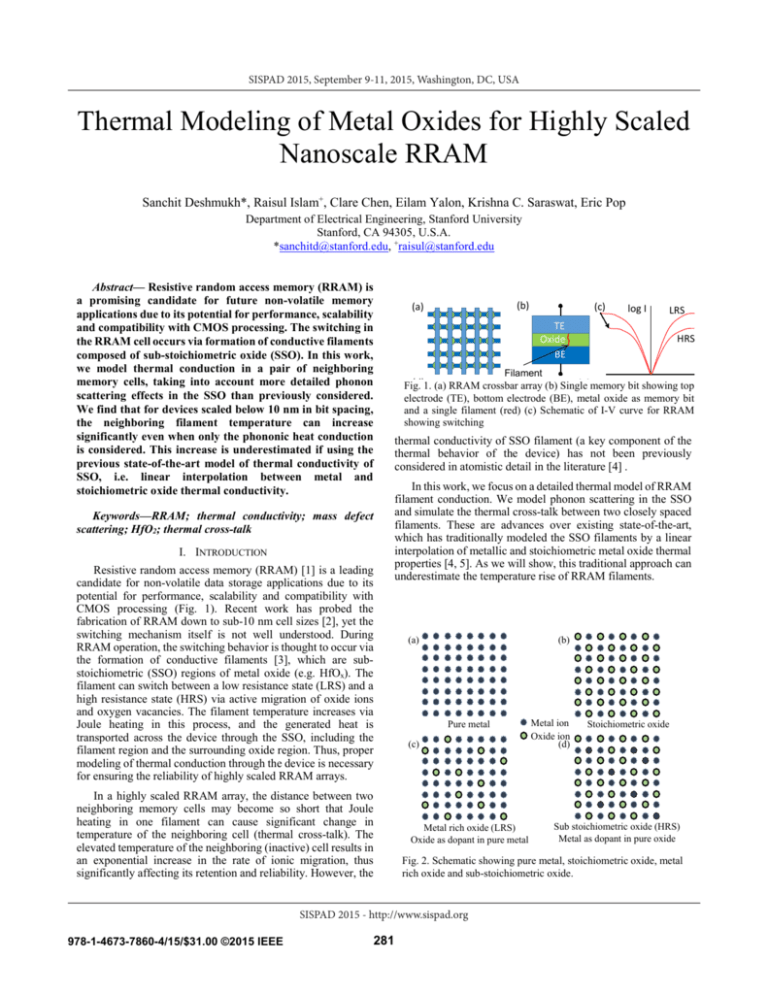
SISPAD 2015, September 9-11, 2015, Washington, DC, USA Thermal Modeling of Metal Oxides for Highly Scaled Nanoscale RRAM Sanchit Deshmukh*, Raisul Islam+, Clare Chen, Eilam Yalon, Krishna C. Saraswat, Eric Pop Department of Electrical Engineering, Stanford University Stanford, CA 94305, U.S.A. *sanchitd@stanford.edu, +raisul@stanford.edu Abstract— Resistive random access memory (RRAM) is a promising candidate for future non-volatile memory applications due to its potential for performance, scalability and compatibility with CMOS processing. The switching in the RRAM cell occurs via formation of conductive filaments composed of sub-stoichiometric oxide (SSO). In this work, we model thermal conduction in a pair of neighboring memory cells, taking into account more detailed phonon scattering effects in the SSO than previously considered. We find that for devices scaled below 10 nm in bit spacing, the neighboring filament temperature can increase significantly even when only the phononic heat conduction is considered. This increase is underestimated if using the previous state-of-the-art model of thermal conductivity of SSO, i.e. linear interpolation between metal and stoichiometric oxide thermal conductivity. (b) (a) log I LRS TE Oxide BE HRS Filament (d)1. (a) RRAM crossbar array (b) Single (e)memory bit showing top Fig. electrode (TE), bottom electrode (BE), metal oxide as memory bit and a single filament (red) (c) Schematic of I-V curve for RRAM showing switching thermal conductivity of SSO filament (a key component of the thermal behavior of the device) has not been previously considered in atomistic detail in the literature [4] . Keywords—RRAM; thermal conductivity; mass defect scattering; HfO2; thermal cross-talk I. INTRODUCTION Resistive random access memory (RRAM) [1] is a leading candidate for non-volatile data storage applications due to its potential for performance, scalability and compatibility with CMOS processing (Fig. 1). Recent work has probed the fabrication of RRAM down to sub-10 nm cell sizes [2], yet the switching mechanism itself is not well understood. During RRAM operation, the switching behavior is thought to occur via the formation of conductive filaments [3], which are substoichiometric (SSO) regions of metal oxide (e.g. HfOx). The filament can switch between a low resistance state (LRS) and a high resistance state (HRS) via active migration of oxide ions and oxygen vacancies. The filament temperature increases via Joule heating in this process, and the generated heat is transported across the device through the SSO, including the filament region and the surrounding oxide region. Thus, proper modeling of thermal conduction through the device is necessary for ensuring the reliability of highly scaled RRAM arrays. In a highly scaled RRAM array, the distance between two neighboring memory cells may become so short that Joule heating in one filament can cause significant change in temperature of the neighboring cell (thermal cross-talk). The elevated temperature of the neighboring (inactive) cell results in an exponential increase in the rate of ionic migration, thus significantly affecting its retention and reliability. However, the In this work, we focus on a detailed thermal model of RRAM filament conduction. We model phonon scattering in the SSO and simulate the thermal cross-talk between two closely spaced filaments. These are advances over existing state-of-the-art, which has traditionally modeled the SSO filaments by a linear interpolation of metallic and stoichiometric metal oxide thermal properties [4, 5]. As we will show, this traditional approach can underestimate the temperature rise of RRAM filaments. (a) (b) Pure metal (c) Metal rich oxide (LRS) Oxide as dopant in pure metal 281 Metal ion Oxide ion (d) Stoichiometric oxide Sub stoichiometric oxide (HRS) Metal as dopant in pure oxide Fig. 2. Schematic showing pure metal, stoichiometric oxide, metal rich oxide and sub-stoichiometric oxide. SISPAD 2015 - http://www.sispad.org 978-1-4673-7860-4/15/$31.00 ©2015 IEEE (c) II. MODELING OF THERMAL CONDUCTIVITY A. Debye Model for Thermal Conductivity We treat the sub-stoichiometric metal oxide filament (MOx) as an alloy of the metal (e.g. M = Hf) and the stoichiometric oxide (e.g. MO2 = HfO2). To model the phonon thermal conductivity in these materials, we use the Glassbrenner [6] approach: = ( + ) + ; = ℏ (1) (2) The Debye temperature Θ and the speed of sound in sub-stoichiometric MOx are assumed to be a weighted interpolation of the metal and stoichiometric MO2 values using the virtual crystal approximation. This approximation has been successfully used in the past for the speed of sound in SiGe alloys with varying proportions of Si and Ge [7]. The interpolation assumes a weighted average of the phonon dispersion for every stoichiometry at each wave vector in momentum space. This is illustrated in Fig. 2, and the resulting speed of sound and Debye temperature interpolations are direct results of this assumption. B. Scattering Rates for Phonons The scattering time is calculated by Matthiesen’s Rule (2) taking into account boundary scattering time , mass defect x = 0.1 x = 0.9 (3) (4) Here = Σ 1 − / , where is the concentration and mi is the mass of the material i (here M and MO2), and is the average mass of the stoichiometry. ( ) = ( )6 / ( Θ ) is the normalized density of states for phonons. depends on the temperature and Θ for the material. We incorporated the temperature dependence of thermal conductivity and scattering times in our calculations. The boundary scattering is non-negligible for both the case of stoichiometric oxide and the metal-rich oxide. In the case of the stoichiometric oxide, the as-deposited unformed RRAM oxides are typically amorphous, effectively leading to nm-scale grain size. Such small grain size results in substantial phonon scattering. Filaments in an RRAM device can be assumed to be metal rich oxide. Phonon scattering should take into account the dimensions of the filament, with the mean free path for phonons being of the order of the diameter of a single filament. Mass defect (MD) scattering involves modeling the SSO as a material with metal atoms interspersed in an amorphous oxide, as can be seen in Fig. 2. Figure 3 shows the scattering time for two different sub stoichiometric oxides, one is metal rich [Hfx(HfO2)1-x; x = 0.9], and the other is slightly oxygen deficient [Hfx(HfO2)1-x; x = 0.1]. The metal atoms act as scattering defects for phonons travelling in the oxide for the case of the x = 0.1 oxide in the bulk RRAM device. In the case of the metal rich oxide, the amorphous oxide is modeled to scatter phonons by virtue of being present in defects between the metal atoms. In Fig. 3(a) we show the effect of MD scattering with temperature on our material. Umklapp scattering is important for more crystalline materials at high temperatures. For a metal-rich filament material, Umklapp scattering brings down total phononic thermal conductivity at high temperatures. Boundary scattering in the filament is the dominant scattering mechanism within the device for x = 0.9. In accordance with the expectations from scattering mechanisms, we see in Fig. 3(a) the boundary scattering dominates in the case of the x = 0.1 metal deficient oxide. For the filament, the MD scattering dominates at low temperatures, followed by Umklapp scattering which causes increased (b) -1 x = 0.1 x = 0.9 0.95 (a) 4 -1 k (W.m .K ) 5 3 2 Linear Interpolation No mass defect scattering 1 0 0 -1 (a) and, ( ) = ℏ /9 -1 where, ∫ ℏ = (3) and Umklapp scattering time k (W.m .K ) = scattering [8,9] time (4): Stoichiometric Oxide (b) 0.9 Oxygen Deficient Oxide 0.85 Metal Rich Filament 0.8 Model 0.2 0.4 0.6 0.8 1 Proportion of Hf in Hf x(HfO2)(1-x) 0.75 200 400 600 T (K) 800 1000 Fig. 4. Bulk thermal conductivity vs. stoichiometry, with linear interpolation between kHf and kHfO2 (red), phonons only with no mass defect scattering (blue) and phononic model with mass defect scattering (black). (b) Calculated temperature dependence of thermal conductivity for different proportions of Hf and HfO2 in a nanoscale filament. Fig. 3. (a) Dependence of scattering time on temperature and Hf proportion in Hfx(HfO2)1-x for x = 0.1 (blue) and x = 0.9 (red). (b) Dependence of scattering time on phonon frequency for x = 0.1 (blue) and x = 0.9 (red). 282 Fig. 5. Schematic illustration of the pair of RRAM cells simulated in this study. The left cell is under write operation and therefore its filament is the heat source in the simulation. scattering at high temperatures. The scattering times as a function of phonon frequency are displayed in Fig. 3(b). Figure 4 shows the thermal conductivity estimated by our model, considering only the phononic contribution as described above. Figure 4(a) shows the thermal conductivity vs. Hf proportion “x”, illustrating the effect of mass defect scattering in SSOs, up to the bulk metal phononic conductivity. This figure also compares our new model with linear interpolation [4, 5], which does not capture the details of the phonon scattering. Figure 4(b) shows the modeled temperature dependence of the phononic thermal conductivity for three different proportions of x. The slightly oxygen deficient HfOx is for x = 0.1 in the amorphous oxide, and the metal rich filament shows the values for a 2 nm diameter [more boundary scattering than bulk metal shown in Fig. 4(a)] highly sub-stoichiometric (x = 0.9) filament. These are consistent with the stoichiometries modeled in Fig. 3. III. DEVICE SIMULATION USING FINITE ELEMENT MODELING To demonstrate the effect of the difference in thermal conductivity on device performance and reliability, we carried out finite element method (FEM) simulations of a simple pair of Fig. 6. Temperature profile along the x axis shown in Fig. 5. The distance between filaments is 5 nm and 1 V is applied on the left cell. The operating filament and the neighboring filament are highlighted. The black line shows the calculation using the phononic filament model developed in this work. The red line shows the calculation using the linear interpolation model of the thermal conductivity of the filament. Fig. 7. Peak temperature inside operating and neighboring filament for different applied bias, as a function of distance between filaments. Comparison between the proposed model and simple linear interpolation model is shown. RRAM cells assuming cylindrical filaments in the oxide. We focus on the thermal write disturb between neighboring memory cells. The filament material has 90% Hf and 10% HfO2, while surrounding material has 10% Hf and 90% HfO2. The top metal contact is Ti followed by Cu. The bottom metal contact is Cu only. The structure simulated by FEM is shown in Fig. 5. FEM simulation was performed using the commercial software Comsol MultiphysicsTM. In this solver, the Fourier heat transfer equation is solved numerically for each mesh point in the 3-dimensional (3D) structure of the device. The left filament, which acts as the heat source, dissipates power thus representing the memory cell under write operation. The power is determined by the electrical simulation using the resistivity of the filament material. The boundary condition on the top and bottom surfaces of the Cu metal lines is set to room temperature (300 K). No explicit boundary condition was imposed on the other boundaries. However, in the space between the metal lines (see Fig. 5) SiO2 was assumed as the encapsulation material. Fig. 8. Ion hopping probability in neighboring filament as a function of distance between filaments for different applied bias. The activation energy is taken as EA = 0.7 eV [1]. 283 Temperature dependent thermal conductivities are used for the filament and the oxide material. For comparison, in Figs. 6 and 7 we also show the simulated temperature profiles using the linear interpolation of the thermal conductivities [4, 5], which under-estimates the temperatures in an operating device. IV. RESULTS AND DISCUSSION In Fig. 6, we examine the temperature distribution across two nearby RRAM elements. Our model predicts that the temperature profile inside the filament cannot be estimated constant with phononic thermal transport considered. Also, the linear interpolation underestimates the temperature across the device from one filament to the other. Higher temperature, estimated by our model affects the reliability and the retention time of the memory cells. The proposed model is important for analyzing the peak temperature as a function of filament distance. Figure 7 shows the peak temperature (T) of both filaments as a function of distance between them, with varying applied bias. The peak temperature increases rapidly when the distance between filaments becomes shorter than ~20 nm. This means that for highly scaled devices the effect of thermal cross-talk becomes prominent. In addition, we point out the increasing difference in peak temperature between our model and the linear approximation for highly scaled devices with increasing bias. Thus, the effect of mass defect and boundary scattering becomes more prominent on the phonon contribution to thermal conductivity for highly scaled devices, and the linear approximation may provide too optimistic a thermal behavior when the dissipated power starts increasing. The increase in neighboring filament temperature leads to an exponential increase in the probability of O ion diffusion into the filament, which follows an Arrhenius-like dependence on the local temperature. The probability of oxygen ion diffusion in a neighboring filament as a function of filament distance (with activation energy, EA = 0.7 eV [1]) is shown in Fig. 8. Our model indicates that for highly scaled RRAM devices, the ion hopping probability significantly increases. V. CONCLUSION not yet included, but will be the focus of future work. For the stoichiometry change between HfO2 and Hf the electrical conductivity increases by ~1015, whereas the thermal conductivity increases by less than ~102. We therefore expect the electronic component of the thermal conductivity to become dominant at a particular metal-rich (oxygen deficient) stoichiometry. Any lower range of stoichiometry is expected to be dominated by the phononic contribution, which is the key contribution of this work for thermal modeling of RRAM devices. VI. ACKNOWLEDGMENT The authors acknowledge fruitful discussions with Dr. Zuanyi Li regarding different aspects of the simulation. R. Islam was supported by a Stanford Graduate Fellowship. E. Yalon acknowledges partial support from a Fulbright Fellowship. E. Pop aknowledges support from the National Science Foundation (NSF) CAREER Award 1430530. VII. REFERENCES [1] [2] [3] [4] [5] [6] [7] [8] In summary, we incorporated mass defect and boundary scattering effects on thermal conductivity of sub-stoichiometric filaments in RRAM devices for the first time. The contribution of electronic thermal conductivity and an iterative solution between the thermal and electrical behavior of the filament are [9] 284 S. Yu, and H. -S. P. Wong, “A phenomenological model for the reset mechanism of metal oxide RRAM”, IEEE Electron Dev. Lett., vol. 31, no. 12, pp. 1455–1457, Oct. 2010. C.-L. Tsai, F. Xiong, E. Pop, and M. Shim, “Resistive random access memory enabled by carbon nanotube crossbar electrodes”, ACS Nano, vol. 7, no. 6, pp. 5360–5366, May. 2013. D.-H. Kwon et al., “Atomic structure of conducting nanofilaments in TiO2 resistive switching memory”, Nature Nanotechnology, vol. 5, pp. 148– 153, Jan. 2010. M.-J. Lee et al., “A fast, high-endurance and scalable non-volatile memory device made from asymmetric Ta2O5-x/TaO2-x bilayer strcutures”, Nature Materials, vol. 10, pp. 625–630, Jul. 2011. S. Larentis, F. Nardi, S. Balatti, D. C. Gilmer, and D. Ielmini, “Resistive switching by voltage-driven ion migration in bipolar RRAM—part II: modeling”, IEEE Trans. Electron Dev., vol. 59, no. 9, pp. 2468–1475, Jun. 2012. C. J. Glassbrenner, and G. A. Slack, “Thermal conductivity of silicon and germanium from 3 K to the melting point”, Phys. Rev., vol. 134, no. 4A, pp. A1058–A1069, May. 1964. Z. Wang, and N. Mingo, “Diameter dependence of SiGe nanowire thermal conductivity”, Appl. Phys. Lett., vol. 97, p. 101903, Sep. 2010. P. G. Klemens, “The scattering of low-frequency lattice waves by static imperfections”, Proc. Phys. Soc. A, vol. 68, no. 12, pp. 1113–1128, 1955. J. Garg, N. Bonini, B. Kozinsky, and N. Marzari, “Role of disorder and anharmonicity in the thermal conductivity of silicon-germanium alloys: a first-principles study”, Phys. Rev. Lett., vol. 106, no. 4, p. 045901, Jan. 2011.
