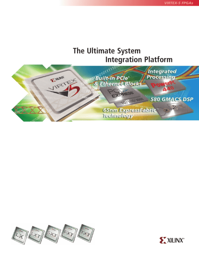
Virtex-5 FPGAs
The Ultimate System
Integration Platform
Comprehen
The Most
In Production now!
One Family—Multiple
Platforms
The Virtex®-5 family of FPGAs offers a choice of five new platforms,
each delivering an optimized balance of high-performance logic,
serial connectivity, signal processing, and embedded processing:
Optimized for high-performance logic
Optimized for high-performance logic with low-power
serial connectivity
Optimized for DSP and memory-intensive applications,
with low-power serial connectivity
Optimized for embedded processing and memory-intensive
applications, with highest-speed serial connectivity
Optimized for ultra high-bandwith applications, such as bridging, switching, and aggregation in wired
telecommunications and data communications systems
All platforms are backed by complete solutions including design
tools, IP, development boards, protocol-specific characterization
reports, training, services, support, and more.
Discover how this new family delivers even higher performance,
lower power, and lower system cost than previous-generation,
Virtex-4 FPGAs.
Optimize I/O Bandwidth, Power and
Cost with Easy-to-Use High-Speed
Serial Solutions
• RocketIO™ GTP transceivers in the LXT and SXT platforms
deliver lowest-power serial connectivity: less than
100 mW (typ) per transceiver at 3.75 Gbps
• RocketIO GTX transceivers in the FXT platform deliver
highest-performance serial connectivity:
150 Mbps – 6.5 Gbps
• First FPGA family with hardened PCI Express® endpoint
blocks and Tri-mode Ethernet MACs
Beat Your Power Budget while
Maximizing Performance
• 35% lower dynamic power with 65nm ExpressFabric
technology and power-saving IP blocks including
PCI Express endpoint, Gigabit Ethernet MAC, and
PowerPC 440 processor
• Further reduce dynamic power consumption by an
average 10% with interactive power analysis tools
• Simplify design with no need to select different power
supply voltages for high performance versus low power
• Reduce system complexity and cost through fewer
power supply rails, fewer regulators, and reduced
board area
Meet Your Performance Targets Easily
• Achieve a two speed-grade performance gain with
new ExpressFabric™ technology
• 550 MHz clocking technology and performance-tuned
IP blocks
• 1.25 Gbps LVDS I/O: up to 600 pin pairs (1,200 I/Os)
• 580 GMACS performance from DSP48E slices
• 190 GFLOPS of single-precision, and 65 GFLOPS of
double-precision floating-point DSP performance
• 1,100 DMIPS per PowerPC® 440 processor block with
high-bandwidth, low-latency interfaces
Virtex-5 FPGAs
Build Highest-Performance
Processing Systems Easily
• Achieve highest throughput with enhanced PowerPC 440
processor block
• Accelerate processing performance with custom co-processors
• Increase DSP algorithm performance with built-in DSP48E slices
nsive 65nm FPGA Solution —
Reduce Cost through System Integration
with Domain-Optimized Platform FPGAs
• Choose a smaller device: 65nm process shrinks die size
and new 6-input LUT increases utilization efficiency
• Meet aggressive performance targets in the least
expensive speed grade
• Reduce part count with built-in, low-power transceivers
• Increase logic efficiency with built-in PCI Express
endpoint and Ethernet MAC blocks
• Integrate embedded processing systems with industrystandard PowerPC 440 processor blocks
• Select smaller heat sinks, fans, and power supplies
enabled by reduced power consumption
• Reduce component cost in volume production
with Virtex®-5 EasyPath™ FPGAs
Bring Your Product to Market Faster with
Proven Development and Verification Tools
• Achieve maximum FPGA performance using ISE® software
featuring Fmax technology and PlanAhead™ design
analysis tools
• Design faster and reduce risk with over 125 pre-verified
IP cores
• Reach timing closure quickly using new SmartCompile
technology that shrinks incremental runtimes
• Optimize designs in less time with SmartXplorer and
ExploreAhead tools that leverage multiple compute platforms
• Speed verification with new FAST simulation models and
IEEE IP encrypted models for hard IP
• Reduce debug cycle time with the real-time verification
capabilities of ChipScope™ Pro tools
• Build complete embedded processing systems with
Platform Studio and Embedded Development Kit
• Implement DSP algorithms modeled using MATLAB® and
Simulink® in custom hardware using System Generator
for DSP
Virtex-5
EasyPath DEVICEs
The conversion-free cost-reduction
path for volume production.
• EasyPath™ devices offer a seamless, low risk
path to volume production that eliminates the
design complexity and the cost of conversion
and re-qualification associated with ASICs and
structured ASICs
• 12 weeks from design completion to
volume production
Finish Your Design Ahead of Schedule with
Expert Training and Services
• Ensure your team has all the tools they need with Xilinx
Productivity Advantage (XPA) Program, a bundled solution
including software, education, and IP cores
• Accelerate product development with Titanium on-site
dedicated engineering from Xilinx
• Ramp your design team with QuickStart!, Xilinx professionally
delivered training coupled with on-site dedicated engineering
• Maintain the flexibility to revert back to standard
Virtex-5 FPGAs if system changes are required.
The
Ultimate System
Integration
65nm ExpressFabric
Technology
Achieve highest performance, most efficient
utilization on 65nm triple-oxide process
• 30% higher speed, 35% lower dynamic power,
and 45% less area than the previous generation
• Industry’s first LUT with six independent inputs
for fewer logic levels
• Flexible LUTs are configurable as logic, distributed
RAM, or shift registers
• Advanced diagonally symmetric interconnect enables shortest,
fastest routing
• From 20,000 to 330,000 logic cells for system-level integration
550 MHz Clocking Technology
Achieve highest speeds with
high-precision, low-jitter clocking
• 12 DCMs provide phase control of less than 30 ps
for better design margin
• 6 PLLs reduce reference clock jitter by more than 2x
• Differential global clocking ensures low skew and jitter
The Right Memory
for Any Application
Distributed RAM—Small
• Build 256-bit memory per CLB
• 64 bits per LUT
550 MHz, 36 Kbit Block RAM—Medium
• Configure Block RAM as multi-rate FIFO
• Built-in ECC for high-reliability systems
• Automatic power conservation circuitry
High-Performance External Memories—Large
• ChipSync™ technology for reliable interfaces
• Achieve data bandwidth up to 389 Gbps Virtex-5 FPGAs
Platform
RocketIO GTP Transceivers:
100 Mbps–3.75 Gbps
Implement serial protocols at
lowest power
RocketIO GTX Transceivers:
150 Mbps–6.5 Gbps
Implement serial protocols at
highest line rates
• Flexible SERDES supports multi-rate
applications
• Designed to work with integrated PCIe®
and Ethernet MAC blocks
• 77% lower power consumption:
less than 100 mW (typ) at 3.75 Gbps
• Cross-platform pin compatibility makes
it easy to migrate to GTX transceivers
for design upgrades
• Flexible SERDES supports multi-rate
applications
• Powerful transmit and receive equalization
techniques (transmit pre-emphasis, receive
linear equalization, and DFE) for best
signal integrity at high line rates
• Integrated “gear box” provides flexible encoding
and saves logic resources: 8b/10b, 64b/66b, and 64b/67b
• Designed to work with integrated PCIe and Ethernet MAC blocks
• Low power consumption: less than 200 mW (typ) at 6.5 Gbps
Sparse Chevron
Packaging Technology
Keep system noise under control
and simplify PCB layout
• Unique PWR/GND pin pattern minimizes
crosstalk and reduces PCB layers
• On-substrate bypass capacitors shrink
PCB area
Enhanced Configuration and
Bitstream Protection
Reduce system cost, increase reliability,
and safeguard your design
• Configure with commodity SPI and parallel flash memory
• Easier partial reconfiguration and smaller frame size
• Greater reliability for in-system reconfiguration with
multi-bitstream management
• Protect your designs with 256-bit AES
(Advanced Encryption Standard) security
PCI Express Endpoint
Block: x1/x4/x8-lane
Reduce power and cost with built-in
support for ubiquitous serial
connectivity standard
• Included on PCI-SIG® integrators list after
successfully completing the rigorous testing
procedures of the Compliance Workshop
• Up to four endpoint blocks
in a single Virtex-5 FXT FPGA
• Works with RocketIO GTP/GTX transceivers
to deliver full PCIe endpoint function
• Built-in hard IP frees user logic resources
and reduces power
Ethernet Media Access
Controller: 10/100/1000 Mbps
Simplify network connectivity with an integrated
tri-mode Ethernet MAC
• UNH-verified compliance
• Up to eight Ethernet MAC blocks in a single device • Built-in hard IP frees user logic resources and reduces power
System Monitor and
Analog-to-Digital
Converter
Simplify system management and diagnostics
• Fully specified 10-bit, 200k samples/s ADC with
programmable monitoring functions (sequencing,
averaging, alarms)
• Simplify the implementation and reduce the cost
of environmental monitoring
• On-chip temperature and supply voltage sensors
• 17 user-selectable external inputs
• Analog measurements accessible via JTAG at any time
550 MHz DSP48E Slice
Achieve up to 580 GMACS performance
using DSP48E slices
IBM PowerPC 440 processor
block with APU Controller and
High-bandwidth Crossbar Switch
Build area-efficient, high-performance embedded
systems with an industry-standard architecture
• 1,100 DMIPS @ 550MHz; achieve 2,200 DMIPS using
a single FPGA with two processors
• Innovative 5x2, 128-bit crossbar switch minimizes
latency and enables point-to-point connectivity
• Simultaneous memory bus and Processor Local Bus
(PLB) access maximizes throughput
• Integrated DMA channels, PLB interfaces, and dedicated
memory interface minimize logic required
• Auxiliary Processor Unit (APU) controller provides
added connectivity for co-processing offload
• 1,056 DSP48E slices in Virtex-5 SX240T device
• Enhanced slice with a 25x18 multiplier, 48-bit adder, and
48-bit accumulator (cascadable to 96 bits) enables singleand double-precision floating-point and high precision
filters with fewer slices
• Configurable for DSP, arithmetic, and bit-wise logic
• Enables efficient adder-chain architectures
• 40% lower power consumption: 1.38mW/100MHz at
a 38% toggle rate
1.25 Gbps SelectIO™ Interface with
ChipSync Source-Synchronous
Technology
Implement industry-standard and custom protocols
• Simplify board design with built-in input delay and
new output delay circuits that compensate for unequal
trace lengths
• Adaptive delay setting recalibrates automatically to
compensate for changing operating conditions
• Interface to popular standards with 1.25 Gbps
differential or 800 Mbps single-ended I/O
• Digitally controlled impedance improves signal integrity,
reduces component count, and shrinks board size
A
Solution for
Design Challenge
Implement Parallel Networking and
System Interface Standards
SelectIO technology, combined with pre-verified IP cores,
make it easy to support all popular interface standards
• 1.25 Gbps LVDS, 800 Mbps single-ended
• Interface or bridge to virtually any external component
• Support multiple electrical standards in the same device with
35 individually configurable I/O banks
• Design with PCI™, RapidIO, XSBI, SPI4.2, and more
• Configure I/Os to support HSTL, LVDS (SDR and DDR), and
more, at voltages from 1.2V to 3.3V
Simplify Source-Synchronous Interfacing
ChipSync technology in every SelectIO technology block provides
precise control over critical timing for high-performance
source-synchronous interfaces
• Achieve performance targets and simplify PCB layout with
flexible per-bit deskew
• Synchronize incoming data to FPGA internal clock with built-in
Serializer/Deserializer
Accelerate Development with Complete
Serial Solutions
Build chip-to-chip, board-to-board, and box-to-box
applications quickly and easily
• Obtain assured compliance with popular standards such as
Gigabit Ethernet, PCI Express, OC-48, XAUI, SRIO, and HD-SDI
• Reduce design time with integrated interface blocks and
pre-verified IP
• Implement custom solutions
• Reduce pin/trace count to simplify board design and reduce
manufacturing cost
• Start designing with ready-to-use solution kits including protocolspecific characterization reports, boards, and simulation models
Bridge Protocols
Protect your investment by interfacing easily to legacy
ASSPs or ASICs
CLK3
µP
CLK4
CLK2
CLK5
CLK1
CLK6
ASSP
• Reduce design time with built-in support for PCI Express and Ethernet
• Implement other popular protocols with pre-verified IP
• Connect external peripheral components to any processor with
standards-compliant I/O
• Virtex-5 TXT devices enable the industry’s first single-FPGA
100G Ethernet MAC solution
Source-Synchronous Interface Support Built into all I/Os
Build Highest-Bandwidth Memory
Interfaces
ChipSync technology and the Memory Interface Generator
tool make it easy to build reliable interfaces to the latest
high-performance memories, including:
Memory
Interface
Data Rate
(Mbps)
Data Width
(# of bits)
Bandwidth
(Gbps)
DDR SDRAM
400
576
230
DDR2 SDRAM
667
576
384
DDR3 SDRAM
800
384
307
QDR II SRAM
600
2 x 324
389
RLDRAM II
600
648
389
Virtex-5 FPGAs
Simplify Protocol Bridging
Every Platform
Build SoC Designs with High-Performance
Create Highest-Performance DSP
Systems
Increase DSP algorithm performance
• Build single or multi-rate filters for high-sample-rate applications
in wireless RF or HD video systems with cascadable DSP48E slices
• Perform fine-granularity data shifting, control, and small bit-width
arithmetic functions efficiently in programmable logic fabric
• Free up DSP processor CPU cycles by off-loading algorithmic-intensive tasks
to the FPGA co-processor
• Obtain highest memory-to-logic ratio with Virtex-5 SXT platform for
efficiently implementing memory-intensive functions in video processing
and medical imaging
Optimize DSP power consumption and cost
• Achieve efficient implementation with Xilinx algorithm/IP core support for
base functions (e.g. FFT, filters), wireless functions (e.g. DDC, DUC, CFR, DPD)
or video/imaging functions (e.g. CODECs)
• Use power-efficient Virtex-5 FPGAs in military manpack or handheld software
defined radios
Build flexible, high-bandwidth interfaces
• Simplify design with built-in support for PCI Express interfaces
• Obtain complete Xilinx solutions for market-specific interfaces such as CPRI™
and OBSAI for wireless or SDI and HD-SDI for professional broadcast systems
• Build high-bandwidth interfaces to DSP processors using Xilinx IP and
reference designs for serial RapidIO, VLYNQ™ interface products, or EMIF
interfaces when using FPGAs as DSP co-processors
Increase DSP Design Productivity
• Develop DSP custom hardware using MATLAB and Simulink design environments
• Accelerate DSP system verification up to 1000x using hardware co-simulation
• Gain immediate FPGA expertise from a Xilinx application specific on-site
engineer, improving your design productivity and accelerating your timeto-market with Titanium Dedicated Engineering.
Embedded Processing
Create customized embedded systems that meet
your unique and exacting requirements
• Integrate high-speed programmable logic with the flexibility of software to optimize performance, power, and cost
• Design system-on-chip functionality with real-time processing capabilities using processor blocks incorporating industry standard PowerPC 440 processor cores built into Virtex-5 FXT devices
• Implement control functions efficiently in all Virtex-5 FPGAs using MicroBlaze™ soft processors
Achieve highest throughput with enhanced
PowerPC 440 processor blocks
• Get non-blocking pipelined point-to-point access to TEMAC, PCIe blocks, and FPGA logic
• Offload PLB with a dedicated memory interface port that
provides up to 128-bit data transfer per cycle
• Maximize data transfer rates with highly pipelined transmit and receive scatter-gather DMA channels
• Optimize system performance through user-selectable port
prioritization and operating frequencies
Accelerate system performance
• Offload CPU-intensive operations such as video processing,
3D data processing, and floating-point math
• Create custom co-processors in the FPGA logic
• Optimize hardware/software partitioning with the PowerPC 440 processor block Auxiliary Processor Unit (APU) controller
• Implement double/single-precision arithmetic operations using IEEE 754-compatible Floating Point Unit option
Embedded PowerPC 440 Processor System Design Example
Streamline Embedded Development and Empower Innovation
System Integration Design Example: Video-Over-IP
• Accelerate processing design with the award winning
Platform Studio tool suite
• Increase productivity with design wizards, customizable IP,
and integrated HW/SW kits
• Simplify system-level debug using Eclipse SDK and ChipScope Pro integrated bus analyzer
• Leverage broad ecosystem support from industry leaders
in real-time O/S, design, debug, and trace technologies
• Provide your team with expert advice and training at the most critical project stage with QuickStart! for Embedded designs
Corporate Headquarters
Xilinx, Inc.
2100 Logic Drive
Implement PCI Express Technology with Reduced
Cost, Power, and Complexity
San Jose, CA 95124
USA
Tel: +1-408-559-7778
Minimize design risk with hardened PCIe blocks for building nextgeneration graphics, storage, networking, and I/O devices
Web: www.xilinx.com
• Integrate multiple functions into a single PCIe technology-enabled FPGA
• Preserve software investment and extend infrastructure life with scalable
bandwidth (x1, x4, x8)
• Re-target designs without changing your PCIe interface implementation as
your project evolves
• Experience a shorter development cycle with QuickStart! for PCIe designs:
an on-site Xilinx dedicated engineer will assist your team with expert
advice and training
Europe
Xilinx Europe
One Logic Drive
Citywest Business Campus
Saggart, County Dublin
Ireland
Tel: +353-1-464-0311
Web: www.xilinx.com
Japan
Xilinx K.K.
Art Village Osaki Central Tower 4F
1-2-2 Osaki, Shinagawa-ku
Tokyo 141-0032 Japan
Tel: +81-3-6744-7777
Web: japan.xilinx.com
Asia Pacific Pte. Ltd.
Xilinx, Asia Pacific
5 Changi Business Park
Singapore 486040
Tel: +65-6407-3000
Web: www.xilinx.com
Application of PCI Express Technology in a Server System
Accelerate development with
ready-to-use solution kits
• Protocol compliance reports
• Device characterization
• Reference designs
• Development boards
• Simulation models
• Pre-verified IP
• Development tools
• User documentation
• Partner solutions
TAKE The
NEXT STEP
Visit us online at www.xilinx.com/virtex5
www.xilinx.com
©2006-2008 Xilinx Inc. All rights reserved. Xilinx,
the Xilinx logo, Virtex, Spartan, ISE, and other
designated brands are trademarks of Xilinx Inc.
CPRI is a trademark of Siemens AG; PCI-SIG,
PCIe, PCI Express, and PCI are trademarks of PCISIG; PowerPC is a trademark of IBM Corp; VLYNQ
is a trademark of Texas Instruments; and are used
with permission. All other trademarks are the
property of their respective owners.
Printed in U.S.A. PN 0010938-7
one
family multiple
Virtex-5 Family
Virtex-5 LX
Virtex-5 LXT
Optimized for High-performance Logic
Optimized for High-performance Logic
with Low-power Serial Connectivity
LX30
Part Number
Memory
Resources
LX85
LX110 LX155 LX220
LX330
XC5VLX85 XC5VLX155 XC5VLX220 XC5VLX220 XC5VLX330
XCE5VLX85 XCE5VLX110 XCE5VLX155 XCE5VLX220
LX20T
XC5VLX20T
LX30T
LX50T
LX85T
XC5VLX30T XC5VLX50T XC5VLX85T
–
–
XCE5VLX330
–
–
–
XCE5VLX85T
Slices 2
4,800
7,200
12,960
17,280
24,320
34,560
51,840
3,120
4,800
7,200
12,960
Logic Cells 3
30,720
46,080
82,944
110,592
155,648
221,184
331,776
19,968
30,720
46,080
82,944
CLB Flip-Flops
EasyPath Cost Reduction Solutions 1
Logic Resources
LX50
XC5VLX30 XC5VLX50
19,200
28,800
51,840
69,120
97,280
138,240
207,360
12,480
19,200
28,800
51,840
Maximum Distributed RAM (Kbits)
320
480
840
1,120
1,640
2,280
3,420
210
320
480
840
Block RAM/FIFO w/ECC (36 Kbits each)
32
48
96
128
192
192
288
26
36
60
108
1,152
1,728
3,456
4,608
6,912
6,912
10,368
936
1,296
2,160
3,888
Digital Clock Manager (DCM)
4
12
12
12
12
12
12
2
4
12
12
Phase Locked Loop (PLL)
2
6
6
6
6
6
6
1
2
6
6
Maximum Single-Ended Pins
400
560
560
800
800
800
1,200
172
360
480
480
Maximum Differential I/O Pairs
200
280
280
400
400
400
600
86
180
240
240
Total Block RAM (Kbits)
Clock
Resources
I/O Resources 4
I/O Standards HT, LVDS, LVDSEXT, RSDS, BLVDS, ULVDS, LVPECL, LVCMOS33, LVCMOS25, LVCMOS18, LVCMOS15, LVCMOS12, LVTTL, PCI33, PCI66,
DSP48E Slices
32
48
48
64
128
128
192
24
32
48
PowerPC 440 Processor Blocks
–
–
–
–
–
–
–
–
–
–
–
PCI Express Endpoint Blocks
–
–
–
–
–
–
–
1
1
1
1
10/100/1000 Ethernet MAC Blocks
–
–
–
–
–
–
–
2
4
4
4
RocketIO GTP Low-Power Transceivers
–
–
–
–
–
–
–
4
8
12
12
Embedded
Hard IP
Resources 5
–
–
–
–
–
–
–
–
–
–
–
-1,-2,-3
-1,-2,-3
-1,-2,-3
-1,-2,-3
-1,-2,-3
-1,-2
-1,-2
-1,-2
-1,-2,-3
-1,-2,-3
-1,-2,-3
Industrial
-1,-2
-1,-2
-1,-2
-1,-2
-1,-2
-1,-2
-1
-1,-2
-1,-2
-1,-2
-1,-2
Configuration Memory (Mbits)
8.4
12.6
21.9
29.2
41.1
53.2
79.8
6.3
9.4
14.1
RocketIO GTX High-Speed Transceivers
Speed Grades
Configuration
Package 6
48
Commercial
23.4
Available
Area
FFA Packages (FF): flip-chip fine-pitch BGA (1.0 mm ball spacing)
FF324
19 x 19 mm
220
220
FF676
27 x 27 mm
400
440
440
440
FF1153
35 x 35 mm
560
560
800
800
FF1760
42.5 x 42.5 mm
800
800
FF323
19 x 19 mm
FF665
27 x 27 mm
FF1156
35 x 35 mm
FF1738
42.5 x 42.5 mm
FF1759
42.5 x 42.5 mm
Notes:
Virtex-5 FPGAs
800
1,200
172 (4)
EasyPath solutions provide a conversion-free path for volume production.
A single Virtex-5 FPGA CLB comprises two slices, with each containing four 6-input LUTs and four Flip-Flops (twice the number found in Virtex-4 FPGA slice),
for a total of eight 6-LUTs and eight Flip-Flops per CLB.
3
Virtex-5 FPGA logic cell ratings reflect the increased logic capacity offered by the new 6-input LUT architecture.
4
Digitally Controlled Impedence (DCI) is available on I/Os of all devices.
5
One system monitor block included in all devices.
6
All products available Pb-free and RoHS compliant packaging.
7
Available I/O for each device-package combination: number of SelectIO interface pins (number of RocketIO transceivers).
1
2
172 (4)
360 (8)
360 (8)
480 (12)
480 (12)
Platforms
Virtex-5 SXT
Virtex-5 FXT
Virtex-5 TXT
Optimized for DSP with
Low-power Serial Connectivity
Optimized for Embedded Processing with
High-speed Serial Connectivity
Optimized for Ultra
High-Bandwidth Applications LX110T LX155T LX220T LX330T SX35T
SX50T
SX95T SX240T
FX30T
FX70T
FX100T FX130T FX200T XC5VTX150T XC5VTX240T
XC5VLX110T XC5VLX155T XC5VLX220T XC5VLX330T XC5VSX35T XC5VSX50T XC5VSX95T XC5VSX240T XC5VFX30T
XC5VFX70T
XC5VFX100T XC5VFX130T XC5VFX200T
XCE5VTX150T
XCE5VTX240T
XCE5VLX110T XCE5VLX155T XCE5VLX220T XCE5VLX330T
–
XC5VFX70T
XC5VFX100T
XC5VFX130T
XC5VFX200T
XCE5VTX150T
XCE5VTX240T
–
XCE5VSX50T XCE5VSX95T XCE5VSX240T
17,280
24,320
34,560
51,840
5,440
8,160
14,720
37,440
5,120
11.200
16,000
20,480
30,720
23,200
37,440
110,592
155,648
221,184
331,776
34,816
52,224
94,208
239,616
32,768
71,680
102,400
131,072
196,608
148,480
239,616
69,120
97,280
138,240
207,360
21,760
32,640
58,880
149,760
20,480
44,800
64,000
81,920
122,880
92,800
149,760
1,120
1,640
2,280
3,420
520
780
1,520
4,200
380
820
1,240
1,580
2,280
1,500
2,400
148
212
212
324
84
132
244
516
68
148
228
298
456
228
324
5,328
7,632
7,632
11,664
3,024
4,752
8,784
18,576
2,448
5,328
8,208
10,728
16,416
8,208
11,664
12
12
12
12
4
12
12
12
4
12
12
12
12
12
12
6
6
6
6
2
6
6
6
2
6
6
6
6
6
6
680
680
680
960
360
480
640
960
360
640
680
840
960
680
680
340
340
340
480
180
240
320
480
180
320
340
420
480
340
340
PCI-X, GTL, GTL+, HSTL I (1.2V, 1.5V, 1.8V), HSTL III (1.5V, 1.8V), HSTL IV (1.5V, 1.8V), SSTL2 I, SSTL2 II, SSTL18 I, SSTL 18 II, DIFF HSTL I, DIFF HSTL II, DIFF SSTL21, DIFF SSTL2 II, DIFF SSTL18 I, DIFF SSTL18 II
64
128
128
192
192
288
640
1,056
64
128
256
320
384
80
96
–
–
–
–
–
–
–
–
1
1
2
2
2
–
–
1
1
1
1
1
1
1
1
1
3
3
3
4
1
1
4
4
4
4
4
4
4
4
4
4
4
4
6
8
4
16
16
16
24
8
12
16
24
–
–
–
–
–
–
–
–
–
–
–
–
–
–
–
8
16
16
20
24
40
48
-1,-2,-3
-1.-2,-3
-1,-2
-1,-2
-1,-2,-3
-1,-2,-3
-1,-2
-1,-2
-1,-2,-3
-1,-2,-3
-1,-2,-3
-1,-2,-3
-1,-2
-1,-2
-1,-2
-1,-2
-1,-2
-1,-2
-1
-1,-2
-1,-2
-1,-2
-1
-1,-2
-1,-2
-1,-2
-1,-2
-1
-1,-2
-1,-2
31.2
43.1
55.2
82.7
13.4
20.1
35.8
79.7
13.6
27.1
39.4
49.3
70.9
43.4
65.8
840 (20)
960 (24)
User I/Os 7
360 (8)
640 (16)
640 (16)
680 (16)
680 (16)
360 (8)
480 (12)
680 (16)
960 (24)
360 (8)
640 (16)
360 (8)
640 (16)
960 (24)
640 (16)
680 (16)
360 (40)
680 (40)
Footprint Compatible Packaging Enables Design
Flexibility
Devices in the same package type are footprint compatible for easy migration across densities and platforms.
You can accommodate changing requirements or implement system upgrades by moving your design
to another pin-compatible device offering a different mix of capabilities, speed, or processing power,
without changing your board layout.
680 (48)
