Odd Number Clock Divider
www.Hardwareguru .com
Odd Number Clock Divider
This question is really common. Design a clock divider that divides by odd number. The following answer shows how to design a divider by 3 which is asymmetrical. The trivial way is to use a state-machine concept; therefore the answer explains state-machine design step-by-step, from functional specifications towards a complete detailed design and implementation.
A functional description of the asymmetrical divider is shown in Figure 1.
Clk
Output
Figure 1: Functional Description of the Divider
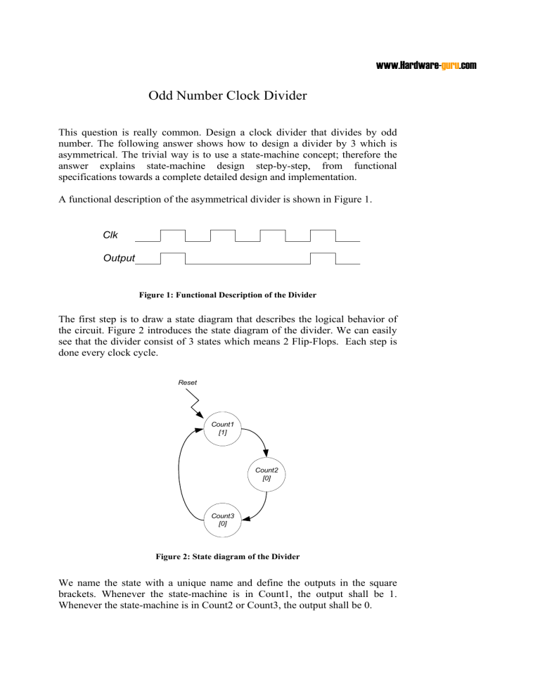
The first step is to draw a state diagram that describes the logical behavior of the circuit. Figure 2 introduces the state diagram of the divider. We can easily see that the divider consist of 3 states which means 2 Flip-Flops. Each step is done every clock cycle.
Reset
Count1
[1]
Count2
[0]
Count3
[0]
Figure 2: State diagram of the Divider
We name the state with a unique name and define the outputs in the square brackets. Whenever the state-machine is in Count1, the output shall be 1.
Whenever the state-machine is in Count2 or Count3, the output shall be 0.
www.Hardwareguru .com
After obtaining the state diagram it is possible to describe the design with a symbolic state transition table. In this step we put all the information we gathered as shown in the following table.
Present State Next Step
Count1
Count2
Count3
Count2
Count3
Count1
Output
1
0
0
Table 1: Symbolic State Transition Table
The next step is to go into details. We have 2 Flip-Flops and one output. This information is entered into an encoded state transition table. The functions can be extracted from a Karnaugh map, or in this case, use the table as a truth table.
Present State
Q0 Q1
0 0
0 1
1 0
Next Step
D0 D1
0
1
0
1
0
0
Output
1
0
0
Table 2: Encoded State Transition Table
We can write the functions as:
• D0 = Q1
• D1 = NOT(Q0+Q1)
• OUT = D1
The implement of the divider by 3 is shown in Figure 3. The output can be connected to Q1 pin.
D
SET
Q D
SET
Q
CLR
Q
Q0
CLR
Q
Q1
Figure 3: Implementation of the Divider
Comments and suggestions: interview@hardware-guru.com
www.Hardwareguru .com

