This is the title
advertisement
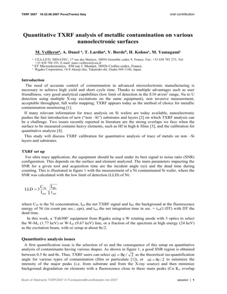
TXRF 2007 18-22.06.2007 Povo(Trento) Italy oral contribution Quantitative TXRF analysis of metallic contamination on various nanoelectronic surfaces M. Veillerota, A. Danel a, T. Lardina, Y. Bordeb, H. Kohnoc, M. Yamagamic a CEA-LETI, MINATEC, 17 rue des Martyrs, 38054 Grenoble cedex 9, France. Fax: +33 438 785 273; Tel: +33 438 784 193; E-mail: marc;veillerot@cea.fr b ST Microelectronics, 850 rue J. Monnet, 38926 Crolles cedex, France. c Rigaku Corporation, 14-8 Akaoji-cho, Takatsuki-shi, Osaka 569-1146, Japan. Introduction The need of accurate control of contamination in advanced microelectronic manufacturing is necessary to achieve high yield and short cycle time. Thanks to multiple advantages such as user friendliness, very good analytical capabilities (low limit of detection in the E10 at/cm2 range, Na to U detection using multiple X-ray excitations on the same equipment), non invasive measurement, acceptable throughput, full wafer mapping; TXRF appears today as the method of choice for metallic contamination monitoring [1]. If many relevant information for trace analysis on Si wafers are today available, nanoelectronic pushes the fast introduction of new (“non –Si”) substrates and layers [2] on which TXRF analysis can be a challenge. Two issues recently reported in literature are the strong overlaps we face when the surface to be measured contains heavy elements, such as Hf in high-k films [3], and the calibration for quantitative analysis [4]. This study will discuss TXRF calibration for quantitative analysis of trace of metals on non –Si layers and substrates. TXRF set up For ultra trace application, the equipment should be used under its best signal to noise ratio (SNR) configuration. This depends on the surface and element analyzed. The main parameters impacting the SNR for a given tool and acquisition time are the incident angle (i) and the dead time during counting. This is illustrated in figure 1 with the measurement of a Ni contaminated Si wafer, where the SNR was calculated with the low limit of detection (LLD) of Ni: LLD 3 C Ni I net I BG t net where CNi is the Ni concentration, Inet the net TXRF signal and IBG the background at the fluorescence energy of Ni (in count par sec.; cps), and tnet the net integration time in sec. = tset(1-DT) with DT the dead time. In this work, a ‘Fab300’ equipment from Rigaku using a W rotating anode with 3 optics to select the W-M (1.77 keV) or W-L (9.67 keV) line, or a fraction of the spectrum at high energy (24 keV) as the excitation beam, with i setup at about c/2. Quantitative analysis issues A first quantification issue is the selection of i and the consequence of this setup on quantitative analysis of contaminants having various shapes. As shown in figure 1, a good SNR region is obtained between 0.5 c and c. Thus, TXRF users can select i c / 2 as the theoretical iso-quantification angle for various types of contamination (film or particulate [1]), or i c / 2 to minimize the intensity of the major peaks (i.e. from substrate and from the X-ray source) and then minimize background degradation on elements with a fluorescence close to these main peaks (Cu K overlap Book of Abstracts TXRF2007 © FondazioneBrunoKessler-irst 2007 session | 1 oral contribution TXRF 2007 18-22.06.2007 Povo(Trento) Italy with the escape peak of W-L as an example). The full extend of this paper will discuss the issue of i selection more in details. The second quantification issue is related to calibration samples. Today, TXRF in IC manufacturing, mainly applied on Si wafers, suffers from the lack of certified standard samples. Calibration must be performed using samples with dried residues (the amount of a given standard element being known) or samples uniformly contaminated, with the level of contamination certified by a reference method, such as VPD-ICPMS. The limitations of these protocols applied to Si and non Si surfaces will be presented in the full extend of the paper. A specific emphasis will be given on the possible use of Si contaminated wafers for the calibration of non Si applications. Signal to noise ratio expressed as the detection limit (at/cm 2) 1.00E+13 1.00E+12 1.00E+11 1.00E+10 0 0.1 best signal to noise ratio 0.2 c 0.3 0.4 0.5 Incident angle (°) Figure 1. Signal to noise ratio obtained on a Ni contaminated Si wafer (31013 Ni at/cm2, W-L excitation). References [1] D. Hellin et al., “Trends in total reflection X-ray fluorescence spectrometry for metallic contamination control in semiconductor nanotechnology”, Spectrochemica Acta part B, 61, (2006), pp. 496. [2] International Technology Roadmaps for Semiconductor industry, http://public.itrs.net, 2005. [3] C. Sparks et al., “Advanced TXRF Analysis: Mapping Metallic Contamination and Background Reduction for Measurements on High-k Materials”, presented at UCPSS 2006, to be published in to be published in Solid State Phenomena 2007. [4] D. Hellin et al., “Determination of metallic contaminants on Ge wafers using direct and droplet sandwich etch TXRF”, Spectrochemica Acta part B, 60, (2005), pp. 209. Book of Abstracts TXRF2007 © FondazioneBrunoKessler-irst 2007 session | 2
