Project Summary – Self Assembly at Photonic and Electronic scales
advertisement
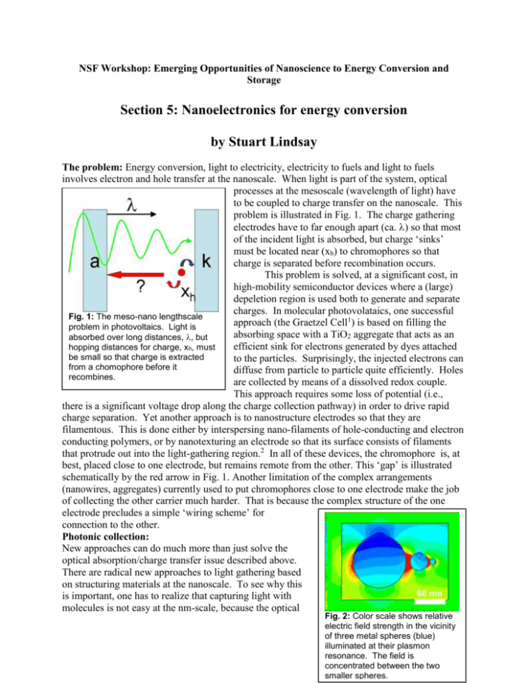
NSF Workshop: Emerging Opportunities of Nanoscience to Energy Conversion and Storage Section 5: Nanoelectronics for energy conversion by Stuart Lindsay The problem: Energy conversion, light to electricity, electricity to fuels and light to fuels involves electron and hole transfer at the nanoscale. When light is part of the system, optical processes at the mesoscale (wavelength of light) have to be coupled to charge transfer on the nanoscale. This problem is illustrated in Fig. 1. The charge gathering electrodes have to far enough apart (ca. ) so that most of the incident light is absorbed, but charge ‘sinks’ must be located near (xh) to chromophores so that charge is separated before recombination occurs. This problem is solved, at a significant cost, in high-mobility semiconductor devices where a (large) depeletion region is used both to generate and separate charges. In molecular photovolataics, one successful Fig. 1: The meso-nano lengthscale approach (the Graetzel Cell1) is based on filling the problem in photovoltaics. Light is absorbing space with a TiO2 aggregate that acts as an absorbed over long distances, , but efficient sink for electrons generated by dyes attached hopping distances for charge, xh, must be small so that charge is extracted to the particles. Surprisingly, the injected electrons can from a chomophore before it diffuse from particle to particle quite efficiently. Holes recombines. are collected by means of a dissolved redox couple. This approach requires some loss of potential (i.e., there is a significant voltage drop along the charge collection pathway) in order to drive rapid charge separation. Yet another approach is to nanostructure electrodes so that they are filamentous. This is done either by interspersing nano-filaments of hole-conducting and electron conducting polymers, or by nanotexturing an electrode so that its surface consists of filaments that protrude out into the light-gathering region.2 In all of these devices, the chromophore is, at best, placed close to one electrode, but remains remote from the other. This ‘gap’ is illustrated schematically by the red arrow in Fig. 1. Another limitation of the complex arrangements (nanowires, aggregates) currently used to put chromophores close to one electrode make the job of collecting the other carrier much harder. That is because the complex structure of the one electrode precludes a simple ‘wiring scheme’ for connection to the other. Photonic collection: New approaches can do much more than just solve the optical absorption/charge transfer issue described above. There are radical new approaches to light gathering based on structuring materials at the nanoscale. To see why this is important, one has to realize that capturing light with molecules is not easy at the nm-scale, because the optical Fig. 2: Color scale shows relative electric field strength in the vicinity of three metal spheres (blue) illuminated at their plasmon resonance. The field is concentrated between the two smaller spheres. absorption cross-section of molecules is much smaller than their physical size. To take a concrete example, the extinction coefficient for the Q-bands of porphyrin (a prototypical chromophore) is 2x10⁴M-1cm-1. Given the maximum possible packing density of these molecules in a monolayer (2.5x10¹³ molecules/cm2), a stack of 2,400 monolayers would be required to Fig. 3: (a) The bacterial photosynthetic complex. Rings labeled LH are the antennas. (b) A synthetic, self-assembled electrode-coupled analog based on a hexagonal, addressable DNA array. Metal spheres (red) are part of a plasmonic antenna system that concentrates light at molecular photovoltaics coupled to a conducting, transparent electrode as shown in (c). Holes are transported to a second electrode by an appropriate redox couple, or possibly by a self-assembled array of holeconducting polymers (red arrows in b). adsorb 99% of the light incident at the Q-band wavelength of 650nm. This is one source of the length-scale problem described above. Photonic assemblies rely on resonant antennas that have much larger optical crosssections than their physical dimensions. These can, in principle, capture light with enormous efficiency (essentially complete absorption in a monolayer) focusing the field to hot spots on the array where chromophores could be placed. Thus a complex light-gathering medium could be replaced with a designed medium that leaves space for the connection of charge carrying wires. An example of such a photonic concentrator was proposed by Li et al.3 and it is illustrated in Fig. 2. It consists of a chain of self-similar spheres, each having the same plasmon resonance frequency, but, because their size changes, essentially all the energy trapped by the larger spehere becomes concentrated in the space between the smaller spheres. The original simulation was based on a solution of the Laplace equation (a static approach) and the simulation shown in Fig. 1 was reworked using a full-physics Maxwell Equation solver (Rudy Diaz – unpublished). The enhancement is reduced compared to the original calculations, but the central point remains valid: light may be gathered much more ‘intelligently’ using engineered nanophotonic structures. But a way is needed to make such structures. Goals for new research Can rationally-designed systems be assembled with critical dimensions at both nano- and mesoscale? This is a key problem in self-assembly.4 We illustrate one approach based on DNAdirected self-assembly in Fig. 3. DNA self-assembly uses the specific base-paring of complementary strands of DNA, combined with DNA’s ability to form three- and four-way junctions to assemble three dimensional nanostructures that can cover macroscopic volumes.5, 6 The proposed technology outlined in Fig. 3 mimics the bacterial photoreaction center (Fig. 3a) by using an antenna structure to gather light, coupling it to a charge-separation device. In this case, the antenna structure consists of a resonant ring of metal spheres, located precisely in space by attachment to a DNA hexagonal lattice (Fig. 3b). The charge separation molecules (detailed in Fig. 3c) are located by the same DNA lattice so that they sit at high field points in the antenna structure. At first sight it might be thought that DNA self-assembly is an outlandish and expensive approach to problems like this. However, even at today’s lab prices, a 100nM synthesis of DNA (costing about $40) would tile twenty four square meters DNA self-assembly is just one approach, used here to illustrate the possibilities. We list below some of the targets for nanoelectronics in this area: Find reliable means for self-assembly at the meso scale (for light gathering) with simultaneous assembly at the nanoscale (for charge gathering). Develop materials for more efficient charge transport. Hopping (electrochemical transport) requires significant driving potential for rapid charge separation, so better molecular ‘wires’ (with enhanced ballistic transport) are needed. Develop rational architectures for collecting electrons and holes: Could electrochemical mediators be replaced with organized ‘wires’ that carry electrons or holes directly to electrodes? Use nano-scale self-assembly to incorporate photonic light-gathering elements into the photovoltaics. Molecular photovoltaics hold out the prospect of low-cost, chemistry-based approaches to energy conversion, but there has been little progress in the 14 years since the first device with significant conversion efficiency was introduced.1 It is time to take a look at fresh approaches in light of recent advances in nanoscience. References 1. O’Regan, B. and M. Grätzel: A low-cost, high-efficiency solar cell based on dyesensitized colloidal TiO2 films, Nature 353, 737–740 (1991). 2. Law, M., L. Greene, J.C. Johnson, R. Saykally, and P. Yang: Nanowire dye-sensitized solar cells, Nature Materials 4, 455-459 (2005). 3. Li, K., M.I. Stockman, and D.J. Bergman: Self-similar chain of metal nanospheres as an efficient nanolens, Phys Rev. Lett. 91, 227402-227401-227404 (2003). 4. Boncheva, M. and G.M. Whitesides: Making things by self-assembly, MRS Bulletin 30, 736-742 (2005). 5. Seeman, N.C.N.: DNA in a material world, 421, 427-431 (2003). 6. He, Y., T. Y., Y. Chen, Z. Deng, A.E. Ribbie, and C. Mao: Sequence symmetry as a tool for designing DNA nanostructures, Angew. Chem. Int. Ed. 44, 6694-6696 (2005).
