Self-assembly of Single Conductive Nanowires at Prescribed Loci
advertisement
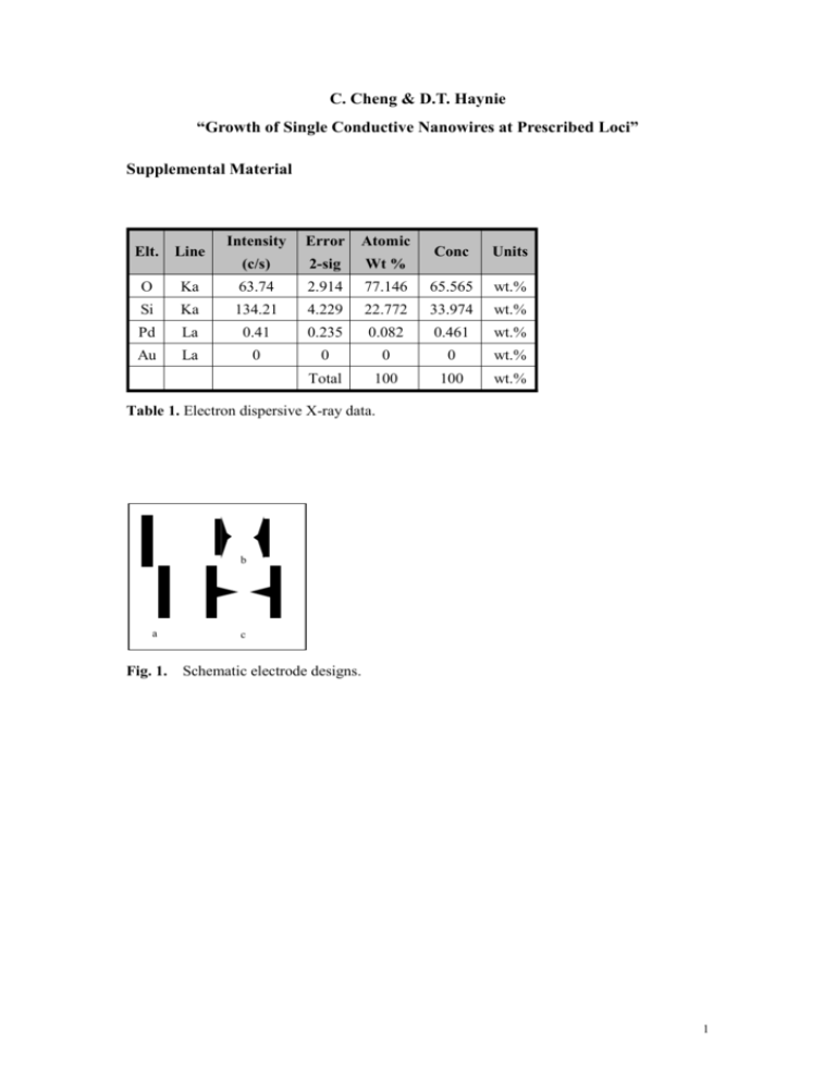
C. Cheng & D.T. Haynie “Growth of Single Conductive Nanowires at Prescribed Loci” Supplemental Material Intensity Error Atomic (c/s) 2-sig Wt % Ka 63.74 2.914 Si Ka 134.21 Pd La Au La Elt. Line O Conc Units 77.146 65.565 wt.% 4.229 22.772 33.974 wt.% 0.41 0.235 0.082 0.461 wt.% 0 0 0 0 wt.% Total 100 100 wt.% Table 1. Electron dispersive X-ray data. b a Fig. 1. c Schematic electrode designs. 1 (a) (b) 2 (c) Fig. 2. Calculated electrical properties of electrode structure (a) in Fig. 1 of supplemental material. (a) Scalar and vector fields. Arrows indicate field magnitude and direction. (b) Equipotential surfaces between electrodes. The direction of the electric field is everywhere perpendicular to an equipotential surface. The magnitude of the field at any point is given by the gradient of the potential. Arrows indicate field magnitude and direction. It is evident from a comparison with Fig. 1(a) and all other electrode structures studied in this work, that nanowires grew at or very close to where the field strength between electrodes was maximal. (c) Density of field lines. 3 (a) (b) Fig. 3. Pt dendritic structures. (a) See Fig. 1(c) for schematic of electrode structure. (b) See Fig. 1(b) for schematic of electrode structure. 4
