Project outline
advertisement
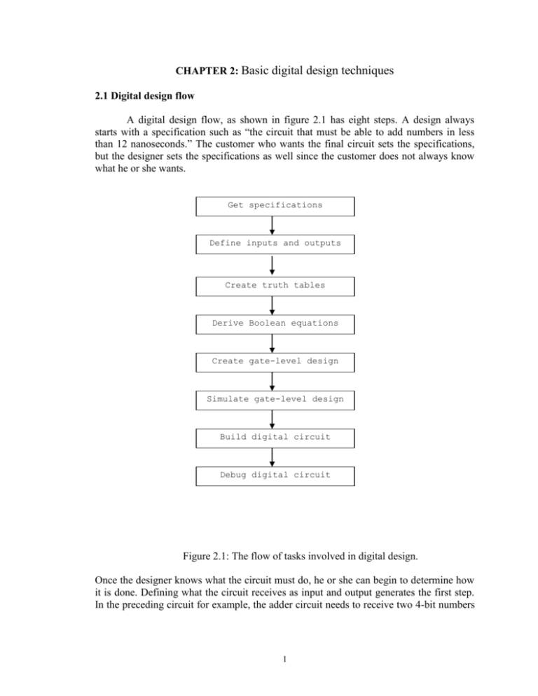
CHAPTER 2: Basic digital design techniques 2.1 Digital design flow A digital design flow, as shown in figure 2.1 has eight steps. A design always starts with a specification such as “the circuit that must be able to add numbers in less than 12 nanoseconds.” The customer who wants the final circuit sets the specifications, but the designer sets the specifications as well since the customer does not always know what he or she wants. Get specifications Define inputs and outputs Create truth tables Derive Boolean equations Create gate-level design Simulate gate-level design Build digital circuit Debug digital circuit Figure 2.1: The flow of tasks involved in digital design. Once the designer knows what the circuit must do, he or she can begin to determine how it is done. Defining what the circuit receives as input and output generates the first step. In the preceding circuit for example, the adder circuit needs to receive two 4-bit numbers 1 as inputs and deliver a 5-bit number as an output. So the adder would have eight binary inputs and five binary outputs. Once the inputs and outputs are known, the designer has to create truth tables, which list what values the outputs will have for each possible combination of input values. To continue with the adder example, if the two 4-bit inputs were 0111 and 1011, then the output would be 10010. This would be one of the many entries in a truth table. Once a truth table is written down, the designer has to derive Boolean equations that describe how each binary output can be computed from the binary inputs using the logical operations of AND, OR and NOT. There is a variety of manual and computer assisted methods to accomplish this step. For an adder example the result of this step would be five Boolean equations employing the eight binary inputs. Next the Boolean equations derived in the previous step are transformed into a gate-level circuit schematic drawing. Each AND, OR and NOT operation in the Boolean equations is replaced with a corresponding AND gate, OR gate or inverter symbol in the schematic. Lines connect the inputs and the outputs of these symbols to represent the passage of binary results between logical operations. Next, the gate level design of the previous step is simulated to check its operation. In its most primitive form, the designer performs simulation. The designer traces various input combinations through the gates of the schematic to determine if the generated output values match the designer’s listed values in the truth table. If the match is okay, then the design will work. If not, then it is necessary to find out where the error was made. Usually, computer simulation is the preferred method as manual simulation is very tedious. Once simulation is competed, the next step is to build a prototype board. Once the board is fabricated, it needs to be tested with test input vectors to see if there were problems with the circuit. 2.2 Combinational Logic Design Techniques Boolean functions are classified into “combinational” or “combinatorial”or “memoryless” and “sequential”. A combinational logic circuit is one whose output depends only on its current inputs. For example the rotary channel selector of an old model TV is a combinational circuit, its “output selects a channel based on the current position of the knob (“input”). The outputs of the sequential function (circuit) depend not only on the current inputs, but also on the past sequence of events, possibly arbitrarily far back in time. The channel selector controlled by the up and down pushbuttons on a TV or VCR is a sequential circuit, the channel selection depends on the up/down pushes. 2 A combinational circuit may contain an arbitrary number of logic gates and inverters but no feedback loops. A feedback loop is the signal path of the circuit that allows the output of a gate/circuit to propagate back to the input of that same gate/circuit; such a loop generally creates a sequential circuit behavior. In combinational circuit analysis, we start with a logic diagram, and proceed to a formal description of the function performed by that circuit, such as a truth table or logic expression. In synthesis, we do the reverse, starting with a formal description and proceeding to a logic diagram. Combinational circuit may have one or more outputs. Most analysis and synthesis techniques can be extended in an obvious way from a single-output to multiple-output circuits. 2.3 Combinational Logic Design Practices A practical combinational circuit may have dozens of inputs and outputs and could require hundreds, thousands, even millions of terms to describe it as a sum of products, and billions of rows to describe in a truth table. Thus, more real combinational logic design problems cannot be solved by application of theoretical techniques, like truth table realization, switching algebra etc. So the usual method of designing such complex circuits is by dividing the whole design into a collection of smaller subsystems, each of which has a smaller description. In combinational logic design, there are several straightforward structures: decoders, multiplexers, and comparators. These structures turn up quite regularly as building blocks in larger systems. These are described in this chapter. But before these can be taken up, it is necessary to know the documentation standards followed by digital designers to ensure that their designs are correct, manufacturable and maintainable. 2.4 Documentation Standards Good documentation of the design is essential for correct design and efficient maintenance of digital systems. In addition to being accurate and complete, documentation must be somewhat instructive, so that a test engineer, maintenance technician, or the original design engineer can figure out how the system works just by reading the documentation. A documentation package should generally contain at least the following five items: Block diagram: A block diagram is an informal pictorial description of the systems major functional modules and their basic interconnections. Schematic diagram: A schematic diagram is a formal description of electrical components of the system, their interconnections, and all of the details needed to construct the system, including IC types, reference designators, and pin numbers. A logic 3 diagram is an informal representation of a design and lacks the level of detail as provided by schematic diagram. Timing diagram: A timing diagram shows the values of various logic signals as a function of time, including the cause-and -effect delays between critical signals. A structured logic description describes the internal function of a standard logic device, such as a programmable logic device(PLD) or a read-only memory (ROM); such a description may be in the form of logic equations, states tables or diagrams, or program listings. A circuit description is a narrative text document that, in conjunction with the other documentation, describes concisely how the circuit is intended to be used and how it works internally. The circuit description should list any assumptions and potential pitfalls in the circuit’s design and operation and point out the use of any non-obvious design “tricks”. 2.5 Commonly Used Logic circuits(components) 2.5.1 Decoders A decoder is a multiple-input logic circuit that converts coded inputs into coded outputs, where the input and output codes are different. The input code generally has fewer bits than the output code, and there is a one-to-one user mapping from input code words into output code words. In a one-to-one mapping, each input code word produces a different output code word. The general structure of a decoder circuit is shown in Fig 2.2. If enable inputs are present, they must be asserted for the decoder to perform its normal mapping function. Decoder Input code word Output code word Enable Inputs Figure 2.2 : Decoder Circuit Structure Otherwise, the decoder maps all input code words into a single “disabled,” output code word. The most commonly used input code is an n-bit binary code, where an n-bit word represents one of 2n different coded values, normally the integers from 0 through 2n-1. Sometimes an n-bit binary code is truncated to represent fewer than 2n values. For 4 example in the BCD code, the 4-bit combinations 0000 through 1001 represent the decimal digits 0-9, and combinations 1010 through 1111 are not used. The most commonly used code is 1-out-of-m code (one hot code), which contains m bits, where one bit is asserted at any time. Thus in a 1-out-of-4 code with active- high outputs, the code words are 0001, 0010, 0100 and 1000. With active low outputs (one cold code), the code words are 1110, 1101, 1011 and 0111. 2.5.2 Binary Decoder The most commonly used decoder circuit is an n-to-2n decoder or binary decoder. Such a decoder has n-bit binary input code and 1-out-of-2n output code. A binary decoder is used when exactly one of 2n outputs, based on n-inputs, needs to be activated. A 2-to-4 decoder is shown below, with its inputs and outputs. 2-to-4 decoder I1 Y0 Y1 Y2 Y3 I2 EN Fig 2.3 2-to-4 Decoder The 74X139 Dual 2-to-4 decoder Two independent and identical 2-to-4 decoders are contained in a single TTL MSI part, the 74x139. The logic symbol for this IC is shown in Figure 2.4 5 74X139 1 1 2 4 1G 1Y0 1A 1Y1 !B 1Y2 2G 1Y3 5 3 15 14 13 6 2Y0 2A 2Y1 2B 7 12 11 10 2Y2 9 2Y3 Fig 2.4: The 74x139 Dual 2-to-4 Decoder Other MSI decoders available are 74x138 3-to-8 decoders. These have three enable inputs, all of which must be asserted for the selected output to be asserted. In addition, multiple decoders can be cascaded to decode larger code words. 2.5.3 THREE-STATE BUFFERS The most basic three-state device is a three-state buffer, often called the threestate driver. The logic symbols for four physically different three-state buffers are shown in Figure 2.5 below. The basic symbol is that of a non-inverting buffer or an inverter. The extra signal at the top of the symbol is an enable input that may be active high or active low. When the enable input is asserted, the device behaves like an ordinary buffer or inverter. When the enable input is negated, the device output “floats”; that is, it goes to a high-impedance (Hi-Z), disconnected state and behaves as if it weren’t even there. (a) (b) (c) (d) Fig 2.5 :Various three state buffers: (a) non-inverting, active-high enable; (b) noninverting, active-low enable; (c) inverting, active-high enable; (d) inverting, active-low enable 6 Three-state devices allow multiple sources to share a single line as long as only one device “talks” on the line at a time. 2.5.4 Standard SSI and MSI Three-state Buffers Like logic gates, several independent three-state buffers may be packaged in a single SSI IC. For example, Fig 2.6 shows the pin-outs of 74x125 and 74x126, each of which contain four independent, non-inverting, three-state buffers in a 14-pin package. The three-state enable inputs in the ‘125 are active low, and in the ‘126 are active high. (1) (13) (3) (12) (1) (11) (2) (10) (4) (6) (9) (13) (3) (12) (11) (10) (4) (8) (5) (6) (9) (8) Fig 2.6: Pin outs of the 74x125 and 74x126 three-state buffers. Mostly many tri-state buffers in an MSI package are enabled or disabled all together. Therefore such tri-state buffer packages have common enable. 2.5.5 Encoders A decoder’s output code normally has more bits than its input code. If the device’s output code has fewer bits than the input code, the device usually called an encoder. The simplest of all encoders is a 2n-to-n, or binary encoder. It has the opposite function as a binary decoder, its input code is the 1-out-of-2n code and its output code is n-bit binary. 2.5.5 Priority Encoders The 1-out-of-2n coded outputs of an n-bit binary decoder are generally used to control a set of 2n devices, where at most one device is supposed to be active at any time. Consider a system with 2n inputs, each of which indicates a request for service. This structure is often used in microprocessor input/output subsystems; where inputs might interrupt requests. In this situation, a binary encoder is used to indicate the input requesting service at any time. However, this encoder works properly only if the inputs are asserted one at a time. 7 When multiple inputs are asserted, the solution is to assign priority to input lines so that only the input line with the highest priority is encoded. Such a device is called a priority encoder. 74x148 is a commercially available, MSI 8-input priority encoder. 2.5.6 Multiplexers A multiplexer is a digital switch. It connects data from one of n sources to its output. A multiplexer is often called MUX for short. Figure 2.7 shows 74x151, an 8input, 1-bit multiplexer. In the above figure, EN stands for enable line. A, B and C are the select inputs. D0, D1 up to D7 are the 8-input data pins. Y and /Y are the outputs of the multiplexer. Four 74x151 multiplexers can be combined to produce a 32-to-1 multiplexer. In addition to these MSI combinational devices, there are adders, subtractors, comparators, multipliers etc. With the logic circuit realizations described in this chapter, it is possible to accomplish any digital system design. 74x151 7 11 10 9 4 3 2 1 15 14 13 12 EN A B C D0 D1 D2 D3 D4 D5 D6 D7 Y Y 5 6 Figure 2.7 : The 74x151 8-input, 1- bit multiplexer The next chapter covers the combinational logic design using Programmable Logic Device(PLD). 8
