5. Object chamber
advertisement
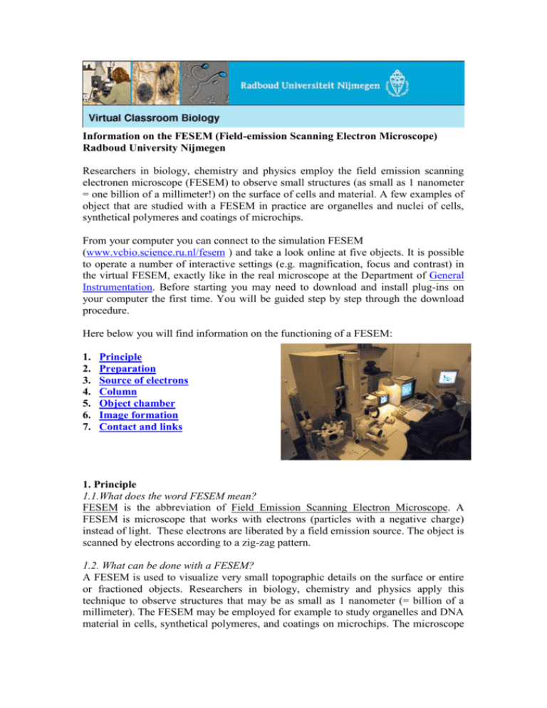
Information on the FESEM (Field-emission Scanning Electron Microscope) Radboud University Nijmegen Researchers in biology, chemistry and physics employ the field emission scanning electronen microscope (FESEM) to observe small structures (as small as 1 nanometer = one billion of a millimeter!) on the surface of cells and material. A few examples of object that are studied with a FESEM in practice are organelles and nuclei of cells, synthetical polymeres and coatings of microchips. From your computer you can connect to the simulation FESEM (www.vcbio.science.ru.nl/fesem ) and take a look online at five objects. It is possible to operate a number of interactive settings (e.g. magnification, focus and contrast) in the virtual FESEM, exactly like in the real microscope at the Department of General Instrumentation. Before starting you may need to download and install plug-ins on your computer the first time. You will be guided step by step through the download procedure. Here below you will find information on the functioning of a FESEM: 1. 2. 3. 4. 5. 6. 7. Principle Preparation Source of electrons Column Object chamber Image formation Contact and links 1. Principle 1.1.What does the word FESEM mean? FESEM is the abbreviation of Field Emission Scanning Electron Microscope. A FESEM is microscope that works with electrons (particles with a negative charge) instead of light. These electrons are liberated by a field emission source. The object is scanned by electrons according to a zig-zag pattern. 1.2. What can be done with a FESEM? A FESEM is used to visualize very small topographic details on the surface or entire or fractioned objects. Researchers in biology, chemistry and physics apply this technique to observe structures that may be as small as 1 nanometer (= billion of a millimeter). The FESEM may be employed for example to study organelles and DNA material in cells, synthetical polymeres, and coatings on microchips. The microscope that has served as an example for the virtual FESEM is a Jeol 6330 that is coupled to a special freeze-fracturing device (Oxford Ato). 1.3. How does a FESEM function? Electrons are liberated from a field emission source and accelerated in a high electrical field gradient. Within the high vacuum column these so-called primary electrons are focussed and deflected by electronic lenses to produce a narrow scan beam that bombards the object. As a result secondary electrons are emitted from ech spot on the object. The angle and velocity of these secondary electrons relates to the surface structure of the object. A detector catches the secondary electrons and produces an electronic signal. This signal is amplified and transformed to a video scan-image that can be seen on a monitor or to a digital image that can be saved and processed further. 1.4. How does een cryo-FESEM look like? A cryo-FESEM looks like a cylindrical column (1) that is mounted on a desk. The column hosts the electron beam. Knobs for the regulation of the electron beam can be found at various levels on the column. There are also tubes present to mainatin the cacuum and the temperature in the instrument and the cryo-unit.The microscope is operated from the steering panel (2; on the desk). A close copy of this panel has been used for the simulations. The cryo-unit with a binocular (3) is located left of the column. When conventional (not cryo) microscopy is applied the exchange chamber in front, below the columns (4) is used to introduce the object into the high vacuum area. The object can be observed on the large screen (5) while it is scanned. The small screen (6) serves to watch the object chamber. The computer for image archiving and processing is located right (7). The cupboards below the desk contain (LOT OF) electronics (8). On the background the sound of the pumps that maintain the vacuum in the caolumsn canbe heared as well as the sissing of the boiling nitrogen for the freeze-unit and the cooling of the column. 2. Preparation In order to be observed with a SEM objects are first made conductive for current. This is done by coating them with an extremely thin layer (1.5 - 3.0 nm) of gold or goldpalladium. Furtheron, objects must be able to sustain the high vacuum and should not alter the vacuum, for example by losing water molecules or gasses. Metals, polymers and crystals are usually little problematic and keep their structure in the SEM. Biological material, however, requires a prefixation, e.g. with cold slush nitrogen (cryo-fixation) or with chemical compounds. This particular microscope is forseen of a special cryo-unit where frozen objects can be fractured and coated for direct observation in the FESEM. Chemically fixed material needs first to be washed and dried below the critical point to avoid damage of the fine structures due to surface tension. Coating is then performed in a separate device. 3. Source of electrons In standard electron microscopes electrons are mostly generated by heating a tungsten filament by means of a current to a temperature of about 2800°C. Sometimes electrons are produced by a crystal of lantanumhexaboride (LaB6) that is mounted on a tungsten filament. This modification results in a higher electron density in the beam and a better resolution than with the conventional device. In a field emission (FE) scanning electron microscope no heating but a so-called "cold" source is employed. An extremely thin and sharp tungsten needle (tip diameter 10–7 –10-8 m) functions as a cathode in front of a primary and secondary anode. The voltage between cathode and anode is in the order of magnitude of 0.5 to 30 KV. Because the electron beam produced by the FE source is about 1000 times smaller than in a standard microscope, the image quality is markedly better. As field emission necessitates an extreme -8 vacuum (10 Torr) in the column of the microscope, a device is present that regularly decontaminates the electron source by a current flash. In contrast to a conventional tungsten filament, a FE tip last theoretically for a lifetime, provided the vacuum is maintained stable. 4. Column with lenses and apertures The electron beam is focused by the electro-magnetic lenses (condenser lens, scan coils, stigmator coils and objective lens) and the apertures in the column to a tiny sharp spot. 1. Condenser lens The current in the condenser determines the diameter of the beam: a low current results in a small diameter, a higher current in a larger beam. A narrow beam has the advantage that the resolution is better, but the disadvantage that the signal to noise ratio is worse. The situation is reversed when the beam has a large diameter. The condenser lens consists mostly out of two parts. 2. Scan coils The scan coils deflect the electron beam over the object according to a zig-zag pattern. The formation of the image on the monitor occurs in synchrony with this scan movement. The scan velocity determines the refreshing rate on the screen and the amount of noise in the image (rapid scan = rapid refreshing = low signal = much noise; see SCANMODE in the virtual FESEM). The smaller the scanned region on the object, the larger the magnification becomes at a constant window size (see MAGNIFICATION in the virtual FESEM). Scan coils often consist of upper and lower coils, which prevent the formation of a circular shadow at low magnification. 3. The objective lens The objective lens is the lowest lens in the column. The objective focuses the electron beam on the object (see FOCUS in the virtual FESEM). At a short working distance (= object in a higher position, that is closer to the objective lens) the objective lens needs to apply a greater force to deflect the electron beam. The shortest working distance produces the smallest beam diameter, the best resolution, but also the poorest depth of field. (The depth of field indicates which range in vertical direction in the object can still be visualized sharply). 4. The stigmator coils The stigmator coils are utilized to correct irregularities in the x and y deflection of the beam and thus to obtain a perfectly round-shaped beam. When the beam is not circular, but ellipsoidal, the image looks blurred and stretched (see ALIGN X Y in the virtual FESEM). 5. Object chamber After the object has been covered by a conductive layer (see preparation) it is mounted on a special holder. The object is inserted through an exchange chamber into the high vacuum part of the microscope and anchored on a moveable stage. In the virtual FESEM the object can be moved in horizontal and vertical direction on the screen by operating the arrows in the POSITION box. In the real microscope the object can be repositioned in the chamber by means of a joy stick that steers in leftright axis, or forward and backward. In addition, the object can be tilted (e.g. for stereo views), rotated and moved in Z direction (= closer or further away to the objective lens). The “secondary electron emission” detector (scintillator) is located at the rear of the object holder in the chamber. 6. Image formation When the primary probe bombards the object, secondary electrons are emitted from the object surface with a certain velocity that is determined by the levels and angles at the surface of the object. The secondary electrons, which are attracted by the Corona, strike the scintillator (fluorescing mirror) that produces photons. The location and intensity of illumination of the mirror vary depending on the properties of the secondary electrons. The signal produced by the scintillator is amplified and transduced to a video signal that is fed to a cathode ray tube in synchrony with the scan movement of the electron beam. The contrast in the ‘real time’ image that appears on the screen reflects the structure on the surface of the object. Parallel to the analog image, a digital image is generated which can be further processed. 7. Contact en links Management of the real FESEM: Geert-Jan Janssen (former employee: Huub Geurts) Technical specialist Jeol: Rob Fase Development of the virtual FESEM: Jeroen van Beurden Web development: Remco Aalbers Initiation + funds application virtual FESEM project: Jan Derksen Imaging - webpages: Elisabeth Pierson Photography: Gerard Dekkers Links: Article about scanning electron microscopy with drawings: www.sem.com/analytic/sem.htm
