PC Parallel Port Interfacing
advertisement
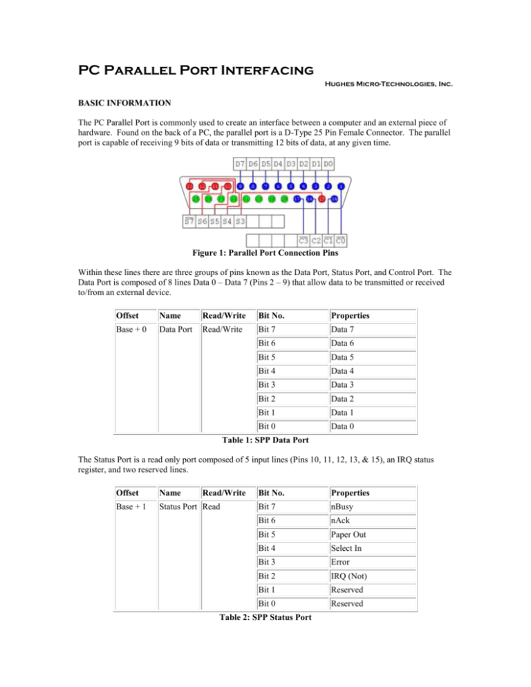
PC Parallel Port Interfacing Hughes Micro-Technologies, Inc. BASIC INFORMATION The PC Parallel Port is commonly used to create an interface between a computer and an external piece of hardware. Found on the back of a PC, the parallel port is a D-Type 25 Pin Female Connector. The parallel port is capable of receiving 9 bits of data or transmitting 12 bits of data, at any given time. Figure 1: Parallel Port Connection Pins Within these lines there are three groups of pins known as the Data Port, Status Port, and Control Port. The Data Port is composed of 8 lines Data 0 – Data 7 (Pins 2 – 9) that allow data to be transmitted or received to/from an external device. Offset Name Read/Write Bit No. Properties Base + 0 Data Port Read/Write Bit 7 Data 7 Bit 6 Data 6 Bit 5 Data 5 Bit 4 Data 4 Bit 3 Data 3 Bit 2 Data 2 Bit 1 Data 1 Bit 0 Data 0 Table 1: SPP Data Port The Status Port is a read only port composed of 5 input lines (Pins 10, 11, 12, 13, & 15), an IRQ status register, and two reserved lines. Offset Name Read/Write Base + 1 Status Port Read Bit No. Properties Bit 7 nBusy Bit 6 nAck Bit 5 Paper Out Bit 4 Select In Bit 3 Error Bit 2 IRQ (Not) Bit 1 Reserved Bit 0 Reserved Table 2: SPP Status Port Finally, the Control Port is composed of 8 lines that are used to control the sending and receiving data. Most importantly is the nStrobe line, which indicates that data is ready to be sent/received. Offset Name Read/Write Bit No. Properties Base + 2 Control Port Read/Write Bit 7 Unused Bit 6 Unused Bit 5 Enable Bidirectional Bit 4 Enable IRQ Bit 3 Select Printer Bit 2 Reset Printer Bit 1 Auto Linefeed Bit 0 nStrobe Table 3: SPP Control Port When writing/reading from the PC Parallel Port it is important to ensure the proper address is being used. Normally the PC Parallel Port is given one of three commonly used base addresses. However, depending on what external devices are active it is easy to confuse the correct address. Address Notes: 0x3BC – 0x3BF Parallel Ports which were incorporated on to Video Cards 0x378 – 0x37 Usual Address For LPT 1 0x278 – 0x27F Usual Address For LPT 2 Table 4: Port Addresses It is also possible to detect the specific address assigned to each individual LPT port within BIOS. For the proper C code to perform this task please visit: http://www.beyondlogic.org/spp/parallel.htm#4 OPERATION MODES Like most devices, the PC Parallel Port has several different modes of operations. These modes range from Standard Mode, which allows for unidirectional operation, to Extended Capabilities Mode (ECP), which allows use of the Extended Capabilities Register (ECR). These modes can be set in BIOS and are described in detail below: Compatibility Mode (Centronics Mode): Compatibility Mode is a unidirectional mode used to send information from the PC to an external device, usually at a rate of approximately 50 KB/s. The process incorporates four steps: 1. 2. 3. 4. The data byte is written to the data lines of the proper parallel port address. A check is made to see if the external device is busy with an operation. The Strobe Line (Pin 1) is pulled low and the data is transferred to the external device. After accepting data, the external device will respond by pulling the nAck Line low for 5 μs. Figure 2: Compatibility Mode Timing Diagram Although Compatibility Mode was intended for unidirectional data transfer, there are several ways to read data from an external device, while in this mode. The first is the use of a bidirectional port, which would require setting the 5th bit in the Control Port to enable this feature. Once this is done, data can be transferred and read by accessing the proper address of the PC Parallel Port. The second method allows for the transfer of 9 bits through the use of nine lines on the Status and Control Ports. External data lines are attached in the displayed manner with several lines using Open Collector Invertors. Open Collector Inverters are used to ensure that the PC Parallel Port can still manipulate the state of each line. Figure 3: External Data Transfer Pin Configuration Once the external logic is prepared, data can be read from the 8 lines, provided that the proper C code is used. The first step requires writing xxxx0100 to the Control Port to enable data transfer. Once this is finished, the data is transferred in two separate nibbles: outportb(CONTROL, inportb(CONTROL) & 0xF0 | 0x04); //Set Control a = (inportb(STATUS) & 0xF0); //Read the MS Nibble a = a |(inportb(CONTROL) & 0x0F); //Read the LS Nibble a = a ^ 0x84; //Combine the MS & LS Nibbles For more information please visit the following link: http://www.beyondlogic.org/spp/parallel.htm#7 Finally, another effective way of reading data from an external device is know as Nibble Mode. Nibble Mode requires the use of a Quad 2 line to 1 line multiplexer. Although Nibble Mode reads the same amount of information as a bidirectional connection or the previous method, it is slower and requires the use of an external IC. The eight data lines of the external device are connected to the A & B input lines of the multiplexer. The outputs of the multiplexer are connected to lines on the Control and Status Ports, as shown below: Figure 4: Pin Connections for Nibble Mode Once again, Nibble Mode requires the use of the proper C code to ensure the data is properly transferred. This time the LS Nibble read first, followed by the MS nibble. Finally, the LS Nibble is shifted and the two are combined: outportb(CONTROL, inportb(CONTROL) | 0x01); //Select LS Nibble(A) a = (inportb(STATUS) & 0xF0); //Read LS Nibble a = a >> 4; //Shift LS Nibble outportb(CONTROL, inportb(CONTROL) & 0xFE); //Select MS Nibble(B) a = a | (inportb(STATUS) & 0xF0); //Read MS Nibble byte = byte ^ 0x88; Combine the MS & LS Nibbles For more information please visit the following link: http://www.beyondlogic.org/spp/parallel.htm#8 Enhanced Parallel Port Mode (EPP) The EPP Mode is far more effective than the Compatibility Mode. Because it uses hardware to generate timing, rather than software, it can reach transfer speeds from 500 KB/s to 2 MB/s. This is the most common mode used for the hobbyist because the EPP Port generates and controls all of the transfers to and from the peripheral. The EPP Mode enables a new set of registers, in addition to the 3 available in Compatibility Mode. These include a new address & data port and several others, summarized in the table below: Address Port Name Read/Write Base + 0 Data Port (SPP) Write Base + 1 Status Port (SPP) Read Base + 2 Control Port (SPP) Write Base + 3 Address Port (EPP) Read/Write Base + 4 Data Port (EPP) Read/Write Base + 5 Undefined (16/32bit Transfers) - Base + 6 Undefined (32bit Transfers) - Base + 7 Undefined (32bit Transfers) - Table 5: EPP Registers In addition, the existing pins on the D-Type 25 Pin Female Connector have different functions when in EPP Mode. The table below summarizes the new functions of each pin: Pin SPP EPP I/O 1 Strobe Write O 2-9 Data 0-7 Data 0-7 10 Ack Interrupt I Interrupt Line 11 Busy Wait I EPP cycle started when low, finished when high. 12 P Out Spare I Spare - Not Used in EPP Handshake 13 Select Spare I Spare - Not Used in EPP Handshake 14 Linefeed Data Strobe O When Low, indicates Data transfer 15 Error Spare I Spare - Note used in EPP Handshake 16 Initialize Reset O Reset - Active Low 17 Select Address Strobe O When low, indicates Address transfer 18-25 Ground Ground Function A low indicates a Write, High indicates a Read I/O Data Bus. Bi-directional Ground Table 6: Pin Assignments For Enhanced Parallel Port Connector. Like the cycles described in the Compatibility Mode section, the EPP Mode requires configuration before a read or write cycle can begin. Again this is accomplished by writing xxxx01000 to the Control Port. A timing diagram for a typical write cycle is shown in the figure below, however, a more detailed description can be found at: http://www.beyondlogic.org/epp/epp.htm Figure 5: EPP Data Write Cycle In this case, a data write statement would require the following steps: 1. 2. 3. 4. 5. 6. 7. The C code write to EPP Data Register 4 (Base +4). The Write line is pulled low indicating a write operation. Data is placed on Data Lines 0-7. The Data Strobe is asserted if Wait is low Host waits for Acknowledgment by Wait going high. Data Strobe is de-asserted. EPP Data Write Cycle Ends. Extended Capabilities Mode (ECP) The ECP Mode has transfer speeds that match that of the EPP Mode, however, it has a few extra features worth noting. ECP Mode uses a FIFO buffer for transferring or receiving data., it uses a real time data compression called Run Length Encoding (RLE) to achieve compression ratios up to 64:1, and it has an Extended Controller Register (ECR) that allows for different operations within ECP Mode. For further details about the capabilities of this PC Parallel Port Mode, please visit the following link: http://www.beyondlogic.org/ecp/ecp.htm

