revised _Supplementary_materials
advertisement

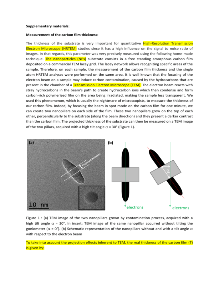
Supplementary materials: Measurement of the carbon film thickness: The thickness of the substrate is very important for quantitative High-Resolution Transmission Electron Microscope (HRTEM) studies since it has a high influence on the signal to noise ratio of images. In that regards, this parameter was very precisely measured using the following home-made technique. The nanoparticles (NPs) substrate consists in a free standing amorphous carbon film deposited on a commercial TEM lacey grid. The lacey network allows recognizing specific areas of the sample. Therefore, on each sample, the measurement of the carbon film thickness and the single atom HRTEM analyses were performed on the same area. It is well known that the focusing of the electron beam on a sample may induce carbon contamination, caused by the hydrocarbons that are present in the chamber of a Transmission Electron Microscope (TEM). The electron beam reacts with stray hydrocarbons in the beam’s path to create hydrocarbon ions which then condense and form carbon-rich polymerized film on the area being irradiated, making the sample less transparent. We used this phenomenon, which is usually the nightmare of microscopists, to measure the thickness of our carbon film. Indeed, by focusing the beam in spot mode on the carbon film for one minute, we can create two nanopillars on each side of the film. These two nanopillars grow on the top of each other, perpendicularly to the substrate (along the beam direction) and they present a darker contrast than the carbon film. The projected thickness of the substrate can then be measured on a TEM image of the two pillars, acquired with a high tilt angle = 30° (Figure 1). (a) (b) α electrons electrons Figure 1 : (a) TEM image of the two nanopillars grown by contamination process, acquired with a high tilt angle = 30°. In insert: TEM image of the same nanopillar acquired without tilting the goniometer ( = 0°). (b) Schematic representation of the nanopillars without and with a tilt angle with respect to the electron beam To take into account the projection effects inherent to TEM, the real thickness of the carbon film (T) is given by: 𝑇= 𝑇𝑚𝑒𝑠 sin 𝛼 Where Tmes and are the projected thickness measured on the TEM images (figure 1a) and the tilt angle (figure 1b) respectivelyThe relative error on the film thickness measurements is given by: ∆𝑇 ∆𝑇𝑚𝑒𝑠 ∆𝛼 = + 𝑇 𝑇𝑚𝑒𝑠 tan 𝛼 We can estimate the error on the measured thickness to be ΔTmes = ± 0.2 nm. During the formation of the contamination pillar, the carbon film may not be perfectly perpendicular to the electron beam inducing an error on the angle estimatedto be Δ± 2.5°. Therefore, the relative error on the film thickness measurements is 16 %. In figure 1, the projected thickness is measured to be 2.5 nm and the real thickness of the carbon film is then 5 ± 0.8 nm. Thickness variations of the carbon film in a range from 5 to 8 nm depending on the analyzed area were measured, but we performed the HRTEM quantitative analyses on the thinnest areas (5 nm) in order to optimize the signal to noise ratio of the single Co and Pt atoms. The results of this original method to precisely measure TEM sample thickness are in good agreement with thickness measurements obtained by the EELS Log-ratio method. We note that heating treatment of the carbon film (75° for 12h) before the metallic vapor phase deposition prevents contamination phenomena during the single atom HRTEM analyses. Time series HRTEM experiments on a 2 nm Pt NPs. (a) (b) (c) (d) Figure 2: Dynamical behaviour of a 2 nm Pt NPs under electron beam irradiation observed at atomic resolution during 15 seconds. As CoPt NPs, pure Pt NPs are stable and maintain their cohesion. Dose-reduced HRTEM analyses. We have performed similar HRTEM analyses of CoPt NPs with a reduced electron dose. As can be seen in figure 3, when reducing the electron dose from 6.5 10 5 e-/nm2 to 6.5 104 e-/nm2, no atomic mobility is observed between the NPs. As the noise level on the carbon film is comparable to the one on images acquired with a higher electron dose, single Co or Pt should be detected if they were on the substrate. We can then assume that the energy transferred to the CoPt NPs does not allow overcoming the energy barrier for atomic evaporation anymore. These reduced dose HRTEM analyses highlights the negligible number of single metal atoms laying around the substrate before beam-induced Ostwald ripening takes place. Accounting for the fast kinetic of single atom diffusion, we can assume that most of the atoms deposited on the substrate during the synthesis are quasi-instantly incorporated into the growing NPs. Figure 3: HRTEM image of CoPt NPs acquired with a reduced electron dose (6.5 104 e-/nm2). Single atoms are not observed on the carbon film.


