experiment 1: introduction to logic design
advertisement
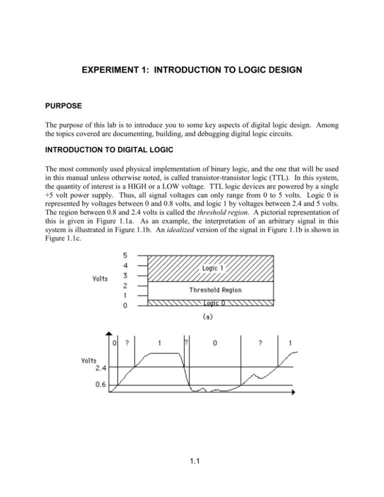
EXPERIMENT 1: INTRODUCTION TO LOGIC DESIGN PURPOSE The purpose of this lab is to introduce you to some key aspects of digital logic design. Among the topics covered are documenting, building, and debugging digital logic circuits. INTRODUCTION TO DIGITAL LOGIC The most commonly used physical implementation of binary logic, and the one that will be used in this manual unless otherwise noted, is called transistor-transistor logic (TTL). In this system, the quantity of interest is a HIGH or a LOW voltage. TTL logic devices are powered by a single +5 volt power supply. Thus, all signal voltages can only range from 0 to 5 volts. Logic 0 is represented by voltages between 0 and 0.8 volts, and logic 1 by voltages between 2.4 and 5 volts. The region between 0.8 and 2.4 volts is called the threshold region. A pictorial representation of this is given in Figure 1.1a. As an example, the interpretation of an arbitrary signal in this system is illustrated in Figure 1.1b. An idealized version of the signal in Figure 1.1b is shown in Figure 1.1c. 1.1 Figure 1.1 Representation of Binary Logic by Voltage Levels. In this type of physical logic system, the higher voltages are usually chosen to correspond to logic 1 and the lower voltages to logic 0. This is called the positive logic convention. If higher voltages are chosen to correspond to logic 0 and lower voltages to logic 1, we have the less common negative logic convention. Note that the choice of logic notation (positive or negative) is merely an assignment of the two voltage levels (HIGH or LOW) to the logic states (0 or 1). Thus, either logic notation can be chosen to describe the same digital circuit. Positive logic will be assumed throughout the rest of this manual unless otherwise mentioned. There are two basic types of elements are used to manipulate logic signals and are also used as building blocks for larger more complex circuits: logic gates and flip-flops. Gates combine one or more logic inputs and from these produce a specified logic output. Flip-flops are storage devices created from gates using feedback. They can be used as memory devices. Circuits that do not exhibit memory are called combinational. They have no flip-flops and generally no feedback. (There are a few unusual cases of circuits that have feedback but do not exhibit memory, and so are considered combinational.) Circuits that exhibit memory are called sequential. They have flip-flops and/or feedback. The symbols representing the most common logic gates, which perform the logical operations AND, OR, NOT, NAND, and NOR, are shown in Figure 1.2. In addition, a table of combinations or truth table, corresponding to each gate is given. The truth table indicates the logic value generated at the output corresponding to all possible combinations of values arriving at the inputs. (Note that a single line entering a circuit is called an input while a pattern of 0s and 1s on all inputs is called an input combination.) For example, consider the two input AND gate of Figure 1.2a. From its truth table in Figure 1.2b, we see that the output C of the AND gate generates logic 1 if and only if logic 1 is present at both of its inputs, A and B. All of these gates, except the inverter, may have more than two inputs (e.g., 3-input gates, 4-input gates and 8-input gates are common). It is important to understand the basic operation of all the logic gates. Take time to learn the operation of gates in Figure 1.2. 1.2 Figure 1.2 Standard Gate Symbols and Truth Tables for Basic Two Input Logic Functions. INTEGRATED CIRCUITS Logic gates, flip-flops, and other digital devices are constructed from integrated circuits (IC's). IC's consist of diodes, transistors, and resistors on a semiconductor base called a chip. Thousands of chips, performing a great variety of logical operations, are available. 1.3 The chip itself is enclosed in a protective metal or plastic case called a package. Connecting pins on the exterior of the package allow input/output signals and power to be transmitted between the chip and the outside world. A common package is the dual in-line package (DIP); in such at package, the connecting pins are arranged in two (dual) lines. The packages commonly have a total of 14, 16, 18, 20, 24, 36, or 40 pins. The pin numbering scheme for 14-, 16-, and 24-pin DIP IC's is shown in Figure 1.3. A notch in the package usually identifies pin 1. (Figure 1.3 shows a top view of the chips. Note that, when viewed from the top, pin 1 is to the left of the notch and when viewed from the bottom, pin 1 is the right of the notch.) Figure 1.3 IC Pin Numberings. (Top View) IC's are classified not only by their logical functions, but also by their logic family. An IC's logic family is determined by the "basic circuit" upon which more complex circuits are based. The most common logic families include TTL--Transistor-transistor logic, ECL--Emitter-coupled logic, MOS--Metal-oxide semiconductor logic, CMOS--Complementary metal-oxide semiconductor logic, and I2L--Integrated-injection logic. Each logic family has its own particular characteristics. Chips from different logic families may not have compatible physical representations of binary 0 and 1; they may use different ranges of voltages for these logical values. Therefore, it is generally not feasible to build a logic circuit out of two or more families of chips. Specification sheets for IC’s list pertinent information regarding the device’s use. These sheets are available in printed data manuals, but most manufacturers of ICs now have these specifications available on the web. For example, the Texas Instrument web site for logic families is http://focus.ti.com/docs/logic/logichomepage.html 1.4 This site has specification sheets for TI’s logic families. For example, if you follow the path ’Data Sheets’, ‘LS’(under select a logic family), ‘SN74LS00’ and ‘Download’ (under the Datasheet section), you will download a data sheet in pdf format for the 74LS00 IC. It is called a quad two-input NAND gate package. This IC contains four, two-input NAND gates, as the name implies. The 54 series number (military grade), 5400, or the 74 series number (commercial grade), 7400 indicate that the chip belongs to the TTL logic family. The pin assignments for the gate inputs, gate outputs, supply voltage, and ground pins are shown at the top left for the 14-pin dual-in-line (DIP) package, the J package. (All the chips used in the 2301 lab are in DIP packages, either 14-pin or 16-pin.) This chip is also available in other packages, e.g., a flatpack package, the fk package. (Another web site containing information on TTL chips is www.datasheets.com.) In addition to pin assignments, the specification sheet gives recommended operating parameters and characteristics for the chip. For example, we see in the Guaranteed Operating Ranges table that, for proper operation, the commercial grade 7400 chip's supply voltage, VCC, should range between 4.75 and 5.25 V. Also from the DC Characteristics over Operating Temperature Range table, we see that an input signal exceeding 2.0 volts, VIH, is guaranteed to be interpreted as HIGH, and one not exceeding 0.8 volts, VIL, as LOW. Similarly, an output is guaranteed to be at least 2.7 volts, VOH, for a HIGH output and less than 0.5 volts, VOL, for a LOW output. CIRCUIT CONSTRUCTION In order to protect the IC's pins and facilitate wiring, the IC's you use will be mounted on a breadboard. An extraction tool, available in the lab, should always be used to remove an IC from its socket; trying to remove them by hand often results in bent and broken IC pins. All IC's should be mounted with the same orientation to facilitate wiring and debugging. It is not advisable to reverse the orientation of some IC's to minimize wire lengths. Wiring is done on the top side of the breadboard, i.e., on the same side that the ICs are inserted; hence, the numbering scheme shown in Figure 1.3 gives the correct view. Appendix A describes the functionality of the logic box available in the lab and how to connect the logic box to the breadboard. The breadboard and ICs used in the experiments are available in the lab kit, available through the bookstore. You should begin connecting your circuits by wiring power, ground, and all unused inputs of gates (for gates having more inputs than needed) to an appropriate constant source. This makes the first connections those that are least likely to change during debugging. Try to keep the wires as close to the surface of the board and as short as possible. Try not to cross too many wires, so that tracing and removal of the wires will be easier. Furthermore, a color code scheme will 1.5 greatly simplify debugging the circuit later. For example, all power supply wires could be red, all ground wires black, etc. When you have finished wiring, examine each pin of each IC to verify its connection. Check all pins without any wires attached to see if they really should have no connection. Be sure to double-check all power connections before applying power to the circuit. The 5 volt power supply provided is short-circuit protected, so that shorting the power supply will merely shut it down until the short circuit is removed. Thus, there is no need to worry about getting a shock from 5 volts. However, you should be concerned about damaging IC's by improper connections! The one sure way to irreparably damage an IC is to reverse power and ground. Most IC's have their ground pin in the lower-left hand corner and power in the upper right-hand corner, when viewed from the bottom. Thus mounting an IC backwards will blow it out. But be alert, some IC's have power and ground in nonstandard locations. Sometimes you will not damage an IC by shorting one of its outputs to ground. However, when a TTL output trying to maintain a LOW level is shorted to the 5 volt power supply, damage will result. Shorting the outputs of CMOS gates to each other, power, or ground for a short period of time is not damaging, but permanent damage may result after a few minutes. Also, if a signal is applied to a CMOS gate input that does not have its power and ground connected, damage may result. Although TTL inputs may be tied directly to ground, they should never be connected directly to the +5 volt power supply. If, by some misfortune, the voltage level at some input terminal exceeds that at the power supply terminal, the chip will be destroyed. Use either a logicbox TTL output to provide a HIGH level to a TTL input, or wire up a gate on your circuit to provide a fixed HIGH level signal at its output to supply the TTL input. (The logic box TTL outputs contain a current limiting resistor in the connection to +5 volts.) DOCUMENTATION The most important prerequisite for good design is good documentation. You should design and document your system completely before you build it, not while you build it. The documentation should include complete circuit diagrams of your system, indicating the part numbers, pin numbers, and physical locations of all the components. Your documentation should generally consist of five parts: a block diagram, logic diagram, chip layout, state diagram, and word description. The block diagram gives an overview of the functional modules comprising the system, while logic diagrams, in conjunction with the chip layout diagram, completely detail the system's construction. State diagrams aid in understanding sequential control circuitry. Finally, the word description should concisely explain the operation of the system and any assumptions made. 1.6 Not all five parts of the documentation are essential for every circuit. For example, simple circuits containing less than 10 IC's may not need block diagrams. The circuit's operation could readily be assimilated from its logic diagram. Also, state diagrams are definitely not applicable to combinational circuits. Block Diagrams In complex systems involving many IC's, a block diagram is essential to attain a fundamental understanding of the system's operation. It must indicate the major subsystems of the system, and the data and control paths between them. In very large systems, additional block diagrams of the individual subsystems may also be required, but there should always be one block diagram illustrating the entire system. The blocks in the diagram indicate functional modules of the system, not the individual components that comprise it. For example, a 16-bit register implemented using four 4-bit registers should be considered as one block rather than four individual blocks. The individual components comprising it are not individually accessible by the other modules. Figure 1.4 illustrates a block diagram. The double arrows indicate buses, i.e., multiple lines used to carry signals, data or control, between modules. It is essential that the flow of control and data between modules in block diagrams be indicated clearly. With control and status lines, the flow is usually in one direction, but lines carrying data, especially buses, are often bidirectional, i.e., the flow can be in both directions. 1.7 Figure 1.4 Example Block Diagram. Logic Diagrams and Chip Layout The logic diagrams and chip layout should give all the information needed to construct the system. The logic diagram should indicate every connection between the components. The chip layout diagram should indicate the position, a reference number (such as U1, U2, etc.), and the part number of each component used in the circuit. Figure 1. illustrates a logic diagram of a circuit. A corresponding chip layout diagram is shown in Figure 1.. Note that NC stands for no connection on the logic diagram. On the logic diagram, the gates and flip-flops used in the circuit should be shown using the standard symbols presented in the introduction to this lab. Each gate and flip-flop should be labeled with the reference number and part number of the IC containing it. In addition, the input and output lines of the gates and flip-flops should be labeled with the corresponding pin numbers on the IC. The gate number on the IC should also be labeled. 1.8 Figure 1.5 Logic Diagram for a Serial Adder. 1.9 Figure 1.6 Chip Layout Diagram for a Serial Adder. Other IC chips should be drawn as rectangles with labels inside denoting their reference and part numbers. Also the names of the input and output pins should be labeled within the rectangle. As with gates and flip-flops, the input/output lines should be labeled with their corresponding pin numbers on the IC to facilitate wiring the circuit. Note that normally power and ground pins for chips are not included in logic diagrams. It is assumed that you can look up their locations from the specification sheets of the IC's. All input and output lines to the circuit must be labeled. It may be helpful to label other lines. DEBUGGING A circuit may sometimes work properly the first time it is turned on, but more likely it will not and, hence, will require debugging. Before power is applied to the circuit, the circuit should be checked to see that it is wired correctly. Improper connections may irreparably damage the chips. (An ohmmeter can be used to check connections if available.) If a connection is missing, check to make sure that it is not simply the result of a misconnected wire by checking the routing of all the other wires leaving the two connection points involved. If, after you apply power, sparks fly, you smell something burning, or one of the chips becomes hot, immediately shut the power off and recheck your circuit. Two types of errors will be detected in debugging: wiring errors and design errors. Both types of errors may be detected by working backwards in the circuit from some point where the erroneous behavior was discovered. If a signal at any point does not have the expected behavior, then work back another level. Do not try to guess the trouble source; such a procedure usually just leads to confusion since the problem is never where you expect it to be. 1.10 The most common wiring errors are omitted and misplaced wires. An omitted wire results in a floating input to a device. A floating TTL input will show a voltage between 1.6 to 1.8 volts, in the threshold region. Misplaced wires sometimes result in short circuits between outputs. Two shorted TTL outputs trying to maintain opposite logic levels will produce an output voltage of about 0.6 volts and may cause damage to one of the driving gates. The most common design errors involve floating unused inputs. Quite often when an input is not used, the designer forgets to make any connection to it. The result is usually an effective logic 1 in TTL circuits however, you cannot depend on this and it is very poor design practice to leave an input unconnected. In CMOS circuits, the effective logic value of the input is indeterminate. Hence all unused inputs should be tied to an appropriate logic source. 1.11 PRELAB 1. Read all of Lab 1 and Appendices A, B and C regarding the logicbox, the oscilloscope, and the computer-aided design (CAD) software, respectively. 2. To acquire proficiency in the documentation of logic circuits, draw a complete logic and chip layout diagram for the logic circuit below (Figure 1.). It is not essential that you understand the operation of this circuit, only the procedures for documenting it. First, construct a complete logic diagram, labeling each gate with its reference and part number. Also be sure to indicate the pin numbers and double check to make sure they are labeled correctly. Next, construct a chip layout diagram. You need to consult the pin assignment diagrams in the data sheets to determine the chip sizes. Try to arrange the chips in an orderly fashion so that those having connections between chips are as near as possible. (Since the breadboards you will use in lab require that the chips be arranged in a single vertical column, use this arrangement for this exercise.) Be sure to label each chip with its reference and part number. If you have any questions regarding the procedures involved in drawing a logic diagram or drawing a chip layout diagram, they can be answered in lab. Make sure to at least attempt to complete these drawings before lab. If no effort is evident, then no credit will be given. Note when constructing the chip layout, you must adhere to the following restrictions: 1) AND gates are available on one 74LS08 chip, 2) XOR gates are available on one 74LS86 chip, 3) Inverters are available on one 74LS04 chip, but 4) the OR gate must be constructed using one AND gate and inverters as needed. X Y OUT1 OUT2 Z Figure 1.7 Schematic Diagram of Logic Circuit for Prelab. 1.12 PROCEDURE Before performing the procedures listed below, read the report section of the experiment to assure you make all required measurements and record all required data. A. Documentation Check 1. Have your TA check your diagrams to ensure that they were done correctly. If you have any questions regarding any aspect of the diagrams, ask your TA now. B. Start-up 1. Familiarize yourself with the front panel controls on the oscilloscope available to you. Refer to Appendix B on the Agilent Technologies MSO-X 2012A Oscilloscope for their functions. 2. Connect the oscilloscope probe to the signal generator with a BNC to BNC cable. You do not need to connect the generator to the logic box. 3. Set the function generator to produce a 5 volt amplitude, 1 kHz sinusoidal wave with no offset. The generator is activated by pressing the LINE pushbutton switch. The generator should be in the "normal" operating mode, indicated by the LED at the upper left hand corner. If not, depress the pushbutton switch immediately below until normal mode is selected. Engage the sine function pushbutton. Press the FREQUENCY button and press the RANGE rocker switch until the LED next to kHz is lit and the decimal point is one digit from the left in the display. Adjust the FREQUENCY vernier until the display reads 1.00 kHz. Make sure the DUTY CYCLE vernier control is pressed in. Press the AMPLITUDE button and adjust the AMPLITUDE control until the display reads 5.00 volts. Make sure the offset switch is in its 12 o'clock position. None of the attenuation or output mode pushbuttons should be engaged. The HORIZONTAL SCALE and VERTICAL SCALE on the scope should be adjusted to produce an appropriate trace. Since the frequency of the sine wave is 1 kHz, 500 s might be a good setting for the HORIZONTAL SCALE. (Recall 1 kHz corresponds to a period of 1/1000 sec. = 1 ms) The five-volt amplitude of the waveform suggests that a 2 VOLTS/DIV for the VERTICAL SCALE might be a good setting for VOLTS/DIV. Also, it is a good idea to establish a ground potential reference level. Adjust the trace by turning the VERTICAL POSITION knob so that the trace is at the desired ground reference level-usually the center of the screen. Observe how the trace moves vertically as the VOLTS/DIV dial is changed. The HORIZONTAL POSITION knob may be used to center the trace horizontally on the display. Use the IntuiLink software to acquire a picture of the oscilloscope display. This procedure is outlined in Appendix B. After obtaining a satisfactory screen image, cut and paste it into your 1.13 final report. Be sure to indicate the ground potential on the display. What is the peak to peak voltage of the waveform? What is its period? Show how you arrived at these figures from the scope display and dial settings. 4. Add a 5 volt offset to the sine wave signal by depressing the OFFSET pushbutton on the function generator and adjusting the OFFSET control until the display reads 5 volts. Record the display and appropriate vernier settings on the scope for both DC and AC couplings. To change the DC/AC coupling setting, press the lit up buttons 1 or 2 and use the button at lower left corner to switch between two couplings. Reconcile the differences between the traces under DC and AC coupling. Be sure to record your ground (0 volts) reference position. 5. Observe a 5 Hz triangle waveform with a 5 volt amplitude, 50% duty cycle, and no offset under both AC and DC coupling. To view this, restore the OFFSET control to its 12 o'clock position. Press the triangle waveform pushbutton. Engage the FREQUENCY pushbutton and adjust the FREQUENCY vernier until the LED displays 5.00 Hz. You will need to adjust the HORIZONTAL SCALE knob until a clear triangle waveform appears. Note that the frequency of this waveform is much smaller than the previous 5 kHz wave. Again reconcile the differences between the DC and AC coupled displays of the signal. 6. Set the function generator to produce a 10 kHz sine wave with a 5 volt amplitude, 50% duty cycle, and no offset. Set the HORIZONTAL SCALE to 50s. Adjust the TRIGGER LEVEL knob and observe the effects on the display. Also try pressing the TRIGGER MENU pushbutton and then the SLOPE softkey at the bottom of the screen. Next change the EDGE SLOPE control along the right side of the screen. How do these controls determine on which part of the cycle of a periodic input signal to trigger, i.e., where in the cycle the trace begins? C. Logic Box Evaluation 1. Connect the logic box to the power supply, then connect the cable from the logic box to the breadboard. If you have any questions about how this is done, consult your TA. 2. Insert a single 74LS00 chip on the breadboard. Connect power and ground to the chip and connect three of the four 2-input NAND gates as shown in the circuit below. Finally connect the clock output from the logic box to the circuit input. Attach one probe from the oscilloscope to the circuit input and the other probe to the circuit output. (Make sure that the ground connector of the probe is connected to the logic ground i.e., the 74LS00 ground pin, not the power supply ground.) Using the oscilloscope capture the circuit input and output waveforms for two different clock signals by selecting two different switch positions. Use MEAS button to obtain the clock frequencies. 1.14 3. Attach an oscilloscope probe to Counter Output #3 from the logic box. Place the counter in the free-running mode and capture the output waveform for both AC and DC coupling. Place the counter in single-step mode and again capture the output waveform for both AC and DC coupling. 1.15 EXPERIMENT 1-- INTRODUCTION TO LOGIC DESIGN FINAL REPORT I. Turn in your Logic and Chip Layout Diagrams. II. Measurements a) Sketch the sine waveform observed in part B.3. VOLTS/DIV_________________ TIME/DIV_________________ b) What is the peak to peak voltage of the waveform? What is its period? What is its frequency? Indicate how you determined these values from the above sketch. 1.16 c) Record the waveforms observed in part B.4. DC Coupling AC Coupling 1.17 d) The waveforms observed using AC and DC coupling are different. Explain why. e) Sketch the waveforms observed on the oscilloscope in part B.5. DC Coupling 1.18 AC Coupling f) Why is the AC coupled trace distorted? g) From your observations in part B.6, explain how the TRIGGER LEVEL knob and the EDGE SLOPE softkeys determine where in the cycle of a periodic input signal the scope begins the trace. 1.19 III. Analysis of Logic Box and Breadboard a) Sketch the input and output waveforms obtained in part C.2 for the two different input frequencies. 1.20 b) Sketch the circuit you constructed showing the pin numbers on each gate. c) What are the frequencies of the input and output waveforms for the two input frequencies you selected? How do the input and output waveforms differ? Is this what was expected? d) Sketch the waveforms obtained in part C.3. Identify the waveforms, i.e., counter was free-running or single stepping and the vertical channel of the scope was in DC or AC mode. 1.21 1.22 e) Does the counter output behave as expected and what is its frequency? What voltages were obtained at the counter output for a logic 0 and logic 1? (Remember that we are using a positive logic convention.) 1.23 f) Explain how the counter output might be used to obtain the table of combinations for a combinational logic circuit. 1.24
