Logic Circuits
advertisement
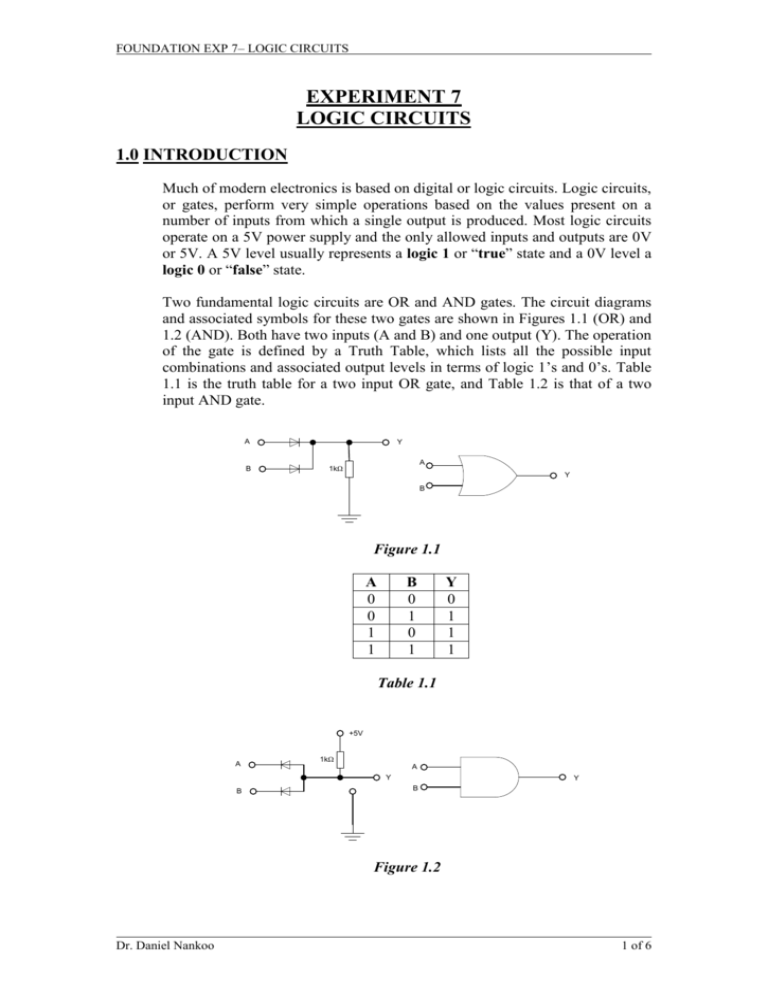
FOUNDATION EXP 7– LOGIC CIRCUITS EXPERIMENT 7 LOGIC CIRCUITS 1.0 INTRODUCTION Much of modern electronics is based on digital or logic circuits. Logic circuits, or gates, perform very simple operations based on the values present on a number of inputs from which a single output is produced. Most logic circuits operate on a 5V power supply and the only allowed inputs and outputs are 0V or 5V. A 5V level usually represents a logic 1 or “true” state and a 0V level a logic 0 or “false” state. Two fundamental logic circuits are OR and AND gates. The circuit diagrams and associated symbols for these two gates are shown in Figures 1.1 (OR) and 1.2 (AND). Both have two inputs (A and B) and one output (Y). The operation of the gate is defined by a Truth Table, which lists all the possible input combinations and associated output levels in terms of logic 1’s and 0’s. Table 1.1 is the truth table for a two input OR gate, and Table 1.2 is that of a two input AND gate. A B Y A 1kΩ Y B Figure 1.1 A 0 0 1 1 B 0 1 0 1 Y 0 1 1 1 Table 1.1 +5V A 1kΩ A Y B Y B Figure 1.2 Dr. Daniel Nankoo 1 of 6 FOUNDATION EXP 7– LOGIC CIRCUITS A 0 0 1 1 B 0 1 0 1 Y 0 0 0 1 Table 1.2 Considering the OR gate, if either input is at logic 1 (or 5V) then the corresponding diode becomes forward biased and starts to conduct. The output voltage will therefore rise to a logic 1 (actually 5V – VF, where VF is the diode forward voltage drop of approx 0.7V). Hence if A OR B is a logic 1 (i.e. ≈ 5V) then the output is a logic 1. If both A and B are at a logic 0 (0V) value neither diode conducts and no voltage appears across the resistor. Considering the AND gate, if either input is at a logic 0 (0V) level the corresponding diode conducts and hence current flows through the resistor and diode causing point Y to fall to a logic 0 (VF ≈ 0.7V) level. Only when A AND B are at a logic 1 level will the output also be at a logic 1 level. 2.0 TESTS 2.1 PROCEDURE 1 Connect up the circuit as shown in Figure 2.1 and connect inputs A, B and C to 0V (logic 0) or 5V (logic 1) in the combinations shown in Table 2.1, which you should draw and complete in your lab book. Measure and record the value of the output (Y) for all possible combinations of the input levels (A, B, C). Use a DMM (set to measure DC voltage) to measure and record the output conditions for all possible combinations, where ≈ 5V level represents a logic 1, and ≈ 0V level represents a logic 0. To generate the inputs A, B, and C, use 5V for logic 1, and 0V for logic 0. Use the variable DC power supply set to 5V for the tests to be carried out in this and the next three procedures. A Y B C 1kΩ V Figure 2.1 Dr. Daniel Nankoo 2 of 6 FOUNDATION EXP 7– LOGIC CIRCUITS A 0 0 0 0 1 1 1 1 B 0 0 1 1 0 0 1 1 C 0 1 0 1 0 1 0 1 Y Table 2.1 Next, connect up the circuit as shown in Figure 2.2 and repeat the above process recording your results in a table similar to Table 2.1 in your lab book. A 1kΩ Y B V C Figure 2.2 2.2 PROCEDURE 2 In practice, logic circuits are normally provided in the form of integrated circuits (i.e. chips). These circuits contain a number of logic gates housed in a single package with a common 0V and 5V supply input. Typical examples are the AND and OR gate packages shown in Figure 2.3. The 74LS08 is a 14 pin integrated circuit chip, consisting of four, 2-input AND gates. Like any electronic device, it requires a source of power to operate. Pin numbers 7 (GND) and 14 (VCC) are the terminals for a power supply to be connected to the chip, where VCC is typically +5V. The pin numbers can be identified by using the small notch or black spot located on top of the chip. Holding the chip with the legs pointing away, and the notch (or black spot) pointing upwards means that pin 1 is at the top left, and pin 14 is at the top right hand corner. As can be seen in Figure 2.3, there are four two-input AND gates. For the first AND gate, its two inputs are at pins 1 and 2, and its output is at pin 3. Dr. Daniel Nankoo 3 of 6 FOUNDATION EXP 7– LOGIC CIRCUITS The 74LS32 is similar to the 74LS08, but consists of four two-input OR gates. Figure 2.3 When connecting chips into your breadboard, you must make use of the central groove of the board. Each side of the chip must occupy sockets on opposing sides of the breadboard. With this in mind, insert the AND (74LS08) package into your breadboard as shown in Figure 2.4 and connect the 0V and 5V power supply links as shown. Connect pins 1 (A) and 2 (B) to 0V (logic 0) or 5V (logic 1) as necessary. Use a DMM set to measure volts to record and measure the output values at pin 3 (Y) with respect to 0V. Present your results in a table in your lab book. Figure 2.4 2.3 PROCEDURE 3 Gates can be in connected to perform very complex operations. As a simple example, consider the electronics to control the opening of a lift door. The door must only be allowed to open if the lift is stationary and at a floor stop (i.e. the doors must not open if the lift stops between floors). In the event of a serious malfunction, a facility must be provided where an “engineer’s key” may be used to open the doors irrespective of the state of the lift. This may be expressed as follows in a logical statement: Dr. Daniel Nankoo 4 of 6 FOUNDATION EXP 7– LOGIC CIRCUITS If lift stopped AND at a valid floor OR if the engineer’s key operated, then open doors. Or in terms of a logic expression: (A AND B) OR C = Y This may be constructed in the form of the logic circuit shown in Figure 2.5. Figure 2.5 In terms of AND and OR gate symbols, the circuit diagram of Figure 2.5 can be redrawn as shown in Figure 2.6. A B C Y Figure 2.6 Using the two logic gate packages, construct the circuit shown in Figure 2.5. In your lab book, draw an appropriate table and record your results for all possible input combinations. 2.4 PROCEDURE 4: TRANSFER CHARACTERISTIC TEST In a computer a change from, say, logic 0 to logic 1 is nearly always considered to be effectively instantaneous. However, in practice the voltage must take some finite time to make this transition, taking all the voltage values between logic 0 and logic 1. In this test the input voltage will be increased in steps from logic 0 to logic 1, and the corresponding output voltages measured. In this test you will need to use two power supplies, but from the same Multi Function bench unit. Use the fixed 5V supply to supply 0V and 5V (logic 0 Dr. Daniel Nankoo 5 of 6 FOUNDATION EXP 7– LOGIC CIRCUITS and logic 1 respectively), and the variable supply to provide the adjustable voltage that will be needed for VC. First test the circuit of Figure 2.1, and then of Figure 2.2. With the circuit of Figure 2.1, set VA = VB = 0V (logic 0), i.e. set them to ground. Vary VC using the variable DC power supply from 0V to 5V (you can see the increments on the power supply’s independent LCD panel, to the left of the power terminals). As you increase VC, take measurements of VC and VY, and tabulate your results. Plot a control graph in the lab, choosing the appropriate axis labelling and scaling, and use it to check whether additional readings are required, especially if you see a bend in the line of your graph. Repeat the above, but this time set VA = VB = 5V (logic 1) – use the fixed 5V supply for these input voltages, and the variable supply for VC. Repeat the above two procedures for the circuit of Figure 2.2. Dr. Daniel Nankoo 6 of 6


