Abstract Template
advertisement
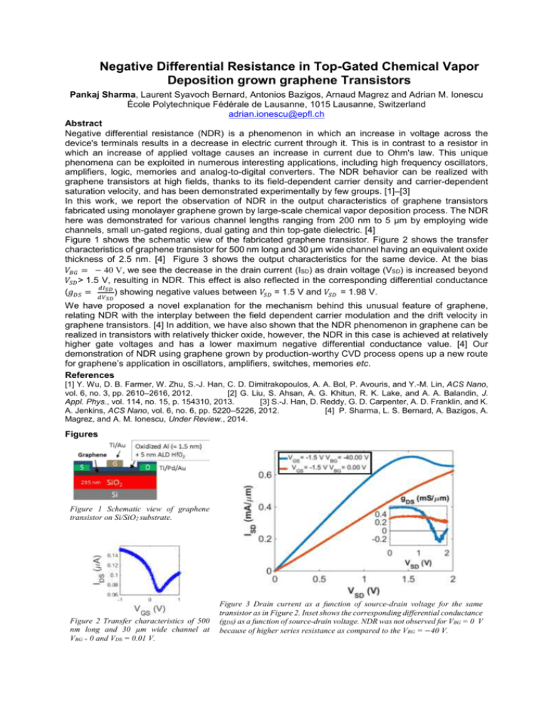
Negative Differential Resistance in Top-Gated Chemical Vapor Deposition grown graphene Transistors Pankaj Sharma, Laurent Syavoch Bernard, Antonios Bazigos, Arnaud Magrez and Adrian M. Ionescu École Polytechnique Fédérale de Lausanne, 1015 Lausanne, Switzerland adrian.ionescu@epfl.ch Abstract Negative differential resistance (NDR) is a phenomenon in which an increase in voltage across the device's terminals results in a decrease in electric current through it. This is in contrast to a resistor in which an increase of applied voltage causes an increase in current due to Ohm's law. This unique phenomena can be exploited in numerous interesting applications, including high frequency oscillators, amplifiers, logic, memories and analog-to-digital converters. The NDR behavior can be realized with graphene transistors at high fields, thanks to its field-dependent carrier density and carrier-dependent saturation velocity, and has been demonstrated experimentally by few groups. [1]–[3] In this work, we report the observation of NDR in the output characteristics of graphene transistors fabricated using monolayer graphene grown by large-scale chemical vapor deposition process. The NDR here was demonstrated for various channel lengths ranging from 200 nm to 5 µm by employing wide channels, small un-gated regions, dual gating and thin top-gate dielectric. [4] Figure 1 shows the schematic view of the fabricated graphene transistor. Figure 2 shows the transfer characteristics of graphene transistor for 500 nm long and 30 µm wide channel having an equivalent oxide thickness of 2.5 nm. [4] Figure 3 shows the output characteristics for the same device. At the bias 𝑉𝐵𝐺 = − 40 V, we see the decrease in the drain current (ISD) as drain voltage (VSD) is increased beyond 𝑉𝑆𝐷 > 1.5 V, resulting in NDR. This effect is also reflected in the corresponding differential conductance 𝑑𝐼𝑆𝐷 (𝑔𝐷𝑆 = ) showing negative values between 𝑉𝑆𝐷 = 1.5 V and 𝑉𝑆𝐷 = 1.98 V. 𝑑𝑉𝑆𝐷 We have proposed a novel explanation for the mechanism behind this unusual feature of graphene, relating NDR with the interplay between the field dependent carrier modulation and the drift velocity in graphene transistors. [4] In addition, we have also shown that the NDR phenomenon in graphene can be realized in transistors with relatively thicker oxide, however, the NDR in this case is achieved at relatively higher gate voltages and has a lower maximum negative differential conductance value. [4] Our demonstration of NDR using graphene grown by production-worthy CVD process opens up a new route for graphene’s application in oscillators, amplifiers, switches, memories etc. References [1] Y. Wu, D. B. Farmer, W. Zhu, S.-J. Han, C. D. Dimitrakopoulos, A. A. Bol, P. Avouris, and Y.-M. Lin, ACS Nano, vol. 6, no. 3, pp. 2610–2616, 2012. [2] G. Liu, S. Ahsan, A. G. Khitun, R. K. Lake, and A. A. Balandin, J. Appl. Phys., vol. 114, no. 15, p. 154310, 2013. [3] S.-J. Han, D. Reddy, G. D. Carpenter, A. D. Franklin, and K. A. Jenkins, ACS Nano, vol. 6, no. 6, pp. 5220–5226, 2012. [4] P. Sharma, L. S. Bernard, A. Bazigos, A. Magrez, and A. M. Ionescu, Under Review., 2014. Figures Figure 1 Schematic view of graphene transistor on Si/SiO2 substrate. Figure 2 Transfer characteristics of 500 nm long and 30 µm wide channel at VBG = 0 and VDS = 0.01 V. Figure 3 Drain current as a function of source-drain voltage for the same transistor as in Figure 2. Inset shows the corresponding differential conductance (gDS) as a function of source-drain voltage. NDR was not observed for VBG = 0 V because of higher series resistance as compared to the VBG = −40 V.
