1 - web page for staff
advertisement
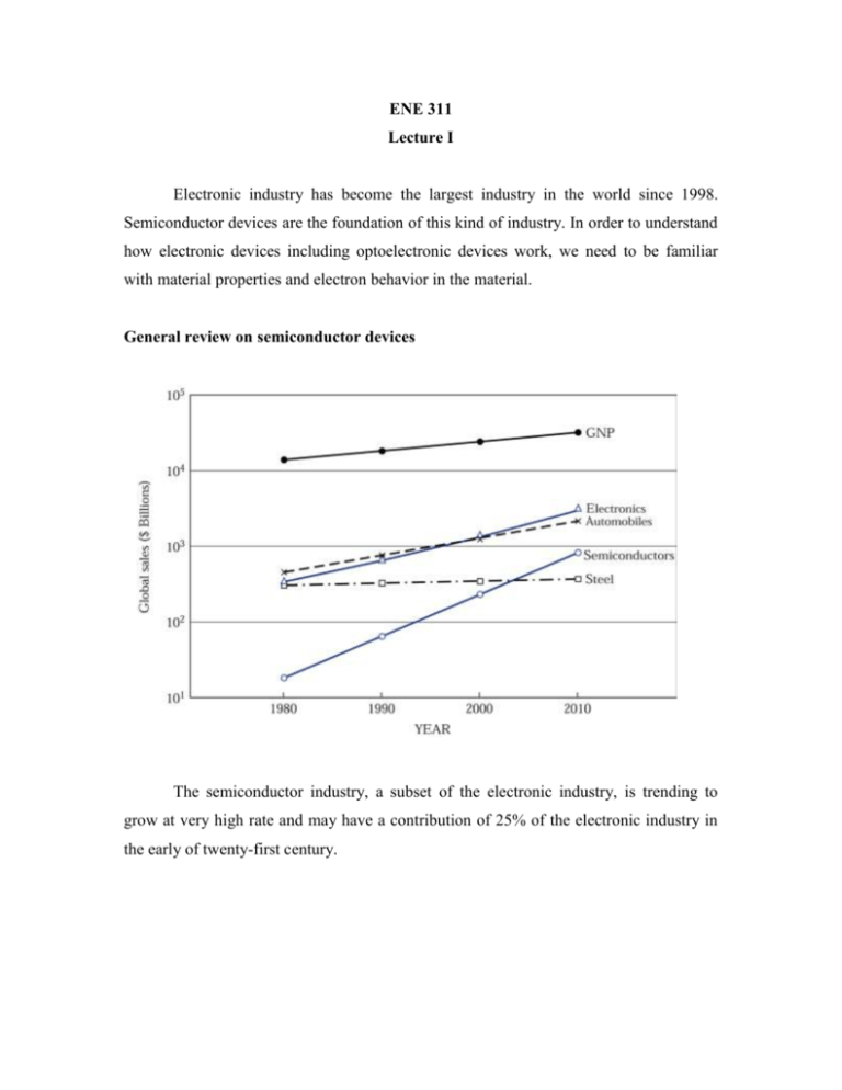
ENE 311 Lecture I Electronic industry has become the largest industry in the world since 1998. Semiconductor devices are the foundation of this kind of industry. In order to understand how electronic devices including optoelectronic devices work, we need to be familiar with material properties and electron behavior in the material. General review on semiconductor devices The semiconductor industry, a subset of the electronic industry, is trending to grow at very high rate and may have a contribution of 25% of the electronic industry in the early of twenty-first century. 2 These are four basic building blocks of semiconductor devices. All semiconductor devices have to be constructed from these mentioned blocks. A metal-semiconductor contact was the first semiconductor device in 1874. This can be used as a rectifying contact* or as an ohmic contact*. We can use this contact in many devices such as MESFET(metal-semiconductor field-effect transistor) where rectifying contact used as a gate and ohmic contacts as a source and a drain. The p-n junction block is formed by putting p-type semiconductor (positively charged carriers) to n-type semiconductor (negatively charged carriers). This p-n junction is a key building block for most semiconductor devices. For example, by adding another p-type semiconductor, p-n-p bipolar transistor can be formed, but if three p-n junctions are used, this can form p-n-p-n device called a thyristor. The heterojunction interface is formed between two different semiconductors. This kind of junction is the key component for high-speed and photonic devices. The last junction is the metal-oxide semiconductor or MOS structure. This structure usually uses with two p-n junctions to form a famous device called MOSFET (MOS field-effect transistor). 3 Semiconductor materials We may group solid-state materials into 3 classes: insulators, semiconductors, and conductors. The factor that is used to separate those materials is called electrical conductivities σ. Insulators have very low conductivities (10-18 – 10-8 S/cm) such as quartz or glass. Conductors have high conductivities (104 – 106 S/cm) such as copper and silver while semiconductors have conductivities between those of insulators and those of conductors. The conductivity of a semiconductor is sensitive to temperature, illumination, magnetic field, and amounts of impurity atoms. This sensitivity makes semiconductor one of the most important materials for electronic applications. 4 If we look at the periodic table, the element semiconductors, such as silicon (Si) or germanium (Ge), can be found in column IV of the table. In the early 1950s, Ge was the most important semiconductor material, but, since the early 1960s, Si has played a major role and virtually displaced Ge as the main material for semiconductor material. The reasons of that are that Si devices give better properties at room temperature and high-quality silicon dioxide (SiO2) can be grown thermally. Si is also second only to oxygen in great quantity. Moreove, devices made from Si cost less than any other semiconductor material and silicon technology is by far the most advanced among all semiconductor technologies. 5 We clearly see a number of important compound semiconductors. There are three kinds of compound semiconductors: binary compound, ternary compound, and quaternary compound. 6 Electrons Electrons behave like a wave and a particle at the same time. There is no theory or experiment to explain electron’s behavior. If we consider electron as a particle, we may start from the study of response of electrons to perturbation such as electric field, magnetic field, or EM waves. Resistivity and Mobility A voltage V is applied across a conductor of length “l” and cross section area “A”. From Ohm’s law: I R l A V R 1 l A where = resistivity [Ω-m] = conductivity [S/m] = 1/ By substitute (2) into (1), we can have (1) (2) 7 I AV l I V A l E J E (3) where V/l = E (electric field) J = current density [A/m2] Under influence of electric field, electron experience a force a eE m (4) where e = electron charge = 1.6 x 10⁻¹⁹ C m = mass of electron a = acceleration Without any applied electric field, the random motion of electron leads to zero net displacement over a long period of time. The average distance between collisions is called the mean free path, and the average time between collisions is called the mean free time, . With applied electric field, electron does not have constant acceleration. It suffers collision that leads it to move with an average velocity called “drift velocity”. A drift velocity can be written as From (4) e vD E m vD e E where µe = mobility of electron [m2/V-s] (5) 8 By moving electrons in conductor, this leads to have a current proportional to number of electrons crossing a unit area [m2] per unit time. J N e .e.vD (6) where Ne = number of free electrons per unit volume From (5) and (6) as electric field E increases, vD also increases, therefore, J also increases. This makes the conductor behave like a perfect source. However, the velocity vD saturates to a maximum value limited by thermal velocity. The mean thermal velocity (vthermal) of electron can be found from 1 2 3 mvthermal kT 2 2 where m = effective mass of electron k = Boltzmann’s constant = 1.38 x 10⁻²³ J/K T = absolute temperature (K) kT/2 = average thermal energy of electron in one-dimension By combining (5) and (6), we have J ( N e e e ) E (7) 9 Comparing (7) to (3), we have N e e e e ( N e e ) (8) where Nee = charge density From (8), the conductivity depends on the charge density and mobility. Metals have high conductivity due to their high density of electrons although their mobilities (μm/t ~ 10 cm2/V-s)are very low compared to those of semiconductors (μS/C ~ 103 cm2/Vs). From (5), the mobility is linearly dependent to the mean free time between collisions which is caused by two major mechanisms: lattice scattering and impurity scattering. Lattice scattering is caused by the thermal vibrations of the lattice atoms at any temperature above absolute zero. As the temperature gets higher, the mobility will get lower. This shows that the mobility will decrease in proportion to T-3/2. Impurity scattering is caused when a charge carrier past an ionized dopant impurity. The carrier will be deflected due to the Coulomb force. The probability of impurity scattering depends on the total concentration of ionized impurities. Unlike, lattice scattering, for impurity scattering, the mobility due to impurity scattering will increase as the temperature gets higher. This mobility in this case is shown to vary as T3/2/NT, where NT is the total impurity concentration. 1 1 L 1 I where µL = mobility due to lattice scattering µI = mobility due to impurity scattering 10 In semiconductors, both electrons and holes contribute to current in the same direction. Hole current and electron current are not necessarily equal because they have different effective masses. J S / C N e e e N h e h E S / C N e e N h h e 11 Ex. Calculate the mean free time of an electron and mean free path having a mobility of 1000 cm2/V-s at 300 K. Assume me = 0.26m0, where m0 = electron rest mass = 9.1 x 10⁻³¹ kg. me e e (0.26 9.1 1031 kg)(1000 104 m 2 .V -1.s -1 ) 1.6 1019 C 0.148 ps From (5), mv 2 3kT 2 2 3kT vth 105 m/s m l vth 14.8 nm s v ; t Ex. In metals, μe = 5 x 10⁻³ m3/(V-s) and l = 1 cm, V = 10 volts is applied. Find the drift velocity vD and compare to thermal velocity vth. V vD e E e l m 2 10 V 5 103 V.s 102 cm vD 5 m/s vth 3kT 3 1.38 10 23 J/K 300K m 9.1 1031 kg vth 1.17 105 m/s vD vth 12 The Hall Effect Assume a p-type semiconductor sample, with electric field applied along xdirection and a magnetic field applied along z-axis, the Lorentz force qv x B (= qvxBz) due to the magnetic filed will exert an average upward force on the holes flowing in the x-direction. Therefore, drifting holes experienced an upward force which deflects holes upward toward the top of the sample and makes them accumulate there. This sets up an electric filed EH in y-direction called “Hall field”. This establishment of the electric field is known as the Hall Effect. At the steady-state, the electric field along the y-axis exactly balances the Lorentz force (or it is called “an equilibrium”); that is qE y qvx Bz or E y vx Bz 13 N h qEH B 1 EH BJ Nhq J N h qv 1 where RH Hall coefficient Nhq This Hall coefficient for n-type semiconductor is similar to the p-type one except it has an opposite sign as RH 1 1 qN e N e e This Hall effect is often used to distinguish an n-type from a p-type sample and also used to calculate the free charge density and the carrier mobility if the conductivity is known. For example, we know that the induced voltage VH known as “Hall Voltage” between the top and bottom is expressed by VH EH d Using a voltmeter to measure VH then VH d I J Wd 1 EH B.J Nee EH VH 1 B.J d Nee BI Ne VH eW If the conductivity σ is known, mobility can be found as ( N e e) e e RH e e RH 14 Ex. A sample of Si is doped with 1016 phosphorus atoms/cm3. Find the Hall voltage in a sample with W = 500 μm, A = 2.5 x 10⁻³ cm2, I = 1 mA, and Bz = 1 Tesla. Note: 1 Tesla = 1 Wb/m2 = 104 G. RH 1 1 625 cm3 / C 19 16 -3 eN e 1.6 10 C 10 cm VH EH d R .I .B RH .J .B d H d A cm3 103 A 104 Wb 625 500 104 cm -3 2 2 C 2.5 10 cm cm VH 1.25 mV
