File
advertisement
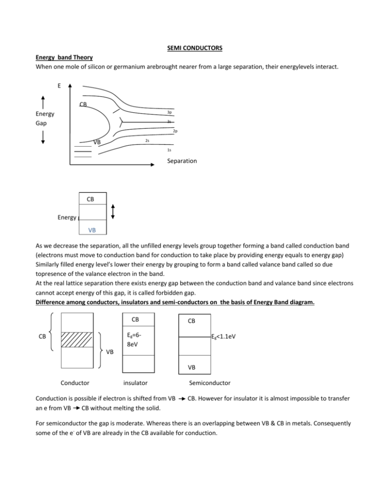
SEMI CONDUCTORS Energy band Theory When one mole of silicon or germanium arebrought nearer from a large separation, their energylevels interact. E CB 3p Energy Gap 3s 2p 2s VB 1s Separation CB CB Energy gap VB As we decrease the separation, all the unfilled energy levels group together forming a band called conduction band (electrons must move to conduction band for conduction to take place by providing energy equals to energy gap) Similarly filled energy level’s lower their energy by grouping to form a band called valance band called so due topresence of the valance electron in the band. At the real lattice separation there exists energy gap between the conduction band and valance band since electrons cannot accept energy of this gap, it is called forbidden gap. Difference among conductors, insulators and semi-conductors on the basis of Energy Band diagram. CB CB Eg=68eV CB Eg<1.1eV VB VB Conductor VB insulator Conduction is possible if electron is shifted from VB an e from VB CB without melting the solid. Semiconductor CB. However for insulator it is almost impossible to transfer For semiconductor the gap is moderate. Whereas there is an overlapping between VB & CB in metals. Consequently some of the e- of VB are already in the CB available for conduction. Concept of Hole as charge Carriers Si o-o Si Si Si As a covalent bond in the silicon lattice is broken, two electrons are released generating two vacancies in the lattice. These vacancies move within the lattice with the help of movement of electrons only,though, in a direction, opposite to direction of motion of electrons. These vacancies are called holes and we recognize them as positive charge carrier’sfree electrons when jump into these holes, energy equal to the energy gap is released and neither the hole nor electron survives. There is a dynamic equilibrium between the number of electrons and number of holes in any semiconductor. The number densityof electrons and holes can be related asne. nh= ni2 Where ni is intrinsic number density Due to formationand breaking of covalent bonds, mobility of hole in less than that of electron 𝑉𝑑 𝜇= 𝐸 Doping:Semiconductors are insulator at room temperature. This is because the energy available at room tem. 300 K is 0.03 eV whereas the energy gap for Si is 1.1 eV and for Ge it is 0.8 eV.Thus at room temperature it’s not possible to shift electron from conduction band to Valence Band. In order to increase the concentration of free electrons and holes to improve conductivity at room temperature, impurities of different kinds are mixed. This is called doping. There are two types of doped or extrinsic semiconductors a) N – type b) P – type N – Type: Si Si Si Ase 0.07eV N type semiconductor is obtained by mixing a pentavalent impurity in the lattice of tetravalent silicon. CB 1.1eV AS-AS---VB Since Arsenic is an electron donorFirst few electronsare in conduction band without any hole in VB. Thus in N – type semiconductor, number of electrons in conduction band number of holes. Energy at room temperature is also equivalent the energy gap between donor level and CB Thus there are a majority of free electrons always available in CB compare to few minority holes in VB.Thus, the name N-type(negative type) is given. P – type: Si Si Si O In0.08eV P type semiconductor is obtained by mixing trivalent impurity in the lattice of tetravalent silicon. The energy required to move the hole within VB is 0.08 eV CB 1.1ev In Accepter level ∑ 0.08 eV In VB First few holes are filled without transferring any e in CB. AS many holes as no. of dopantare generated in VB.After that only e s are shifted to CB.Thus, in P – typeSemiconductor, there is always excess of holes in VB over free electrons in CB.Thus, P-type (positive type) name is given. The 13th group impurity is known as acceptor since it can accept an electron from the lattice. Donors of N- type semiconductor becomes +vely chargedfixed ions after donating electrons to conduction band. Acceptors of P – type semiconductor becomes-velycharged fixed ions after accepting electrons from lattice. Devices a) P n Diode – Di electrode Junction A junction diode is formed by fusing n type semiconductor into p-type semiconductor. Since the concentration of electrons and holes are different across the junction,diffusion current is set up due to the diffusion of electrons from n type to p type and holes from p types to n-type. As the diffusion continues, a +ve sheath of immobile ions and a negative sheath of immobile ions are generated in the vicinity of the function creating a barrier potential across the junction. In equilibrium, the barrier potential is sufficiently large to stop the diffusion of majority charge carriers across the junction. The thin layer across the junction where majority carriers have been depleted out is known as Depletion layer.Order of depletion layer is in micrometer and that of barrier potential is 0.8 volt. P n Vo = 0.8 V p hh hh hh ee ee ee Biasing of diode: Biasing is the process of connecting an external battery with a junction diode. They are of Two types Forward Biasing:- During forward biasing +ive terminal of battery is connected with p type semiconductor. Vb = 0.8 V I forward bias characteristics P n V 0.8 V V (nonohmic) During forward biasing, if applied voltage is more than barrier potential, diffusion current restarts due to diffusion of majority change carriers. Current increasesexponentially due to exponential growth of charge carriers 𝐸𝑔 ) 2𝐾𝑇 n = noexp( Number density at room temperature of that of metal. Eg – Energy gap k – Boltzmannconcept T – Temperature During forward bias, since current is very high, resistance of diode is very low and therefore the diode is in on stage. Backward Biasing (Reverse Biasing) Reverse biasing is the process of connecting – ve terminal of the battery with the p type semiconductor. As the potential difference applied across the junction diode is favoring the barrier potential, Therefore the depletion layer increases. I (mA) P n Avalanche Breakdown knee Voltage Voltage V -V Minority current or tunneling current I (𝜇A) V R V = IR = Constant on breakdownAs the reverse bias voltage increases further, it increases the electric field developed across the depletion layer . A very small current due to transfer of minority charge carriers flows in the order of few micro ampere due to tunneling effect. At a particular reverse biasing voltage called breakdown voltage, the electric field across the junction becomes sufficiently large to rupture the covalent bonds near the junction it is marked by sudden increase in reverse bias current. Such phenomenon is called Avalanche Breakdown. Thus During reverse bias before breakdown, diode is off as current is very low and resistance is very high. After breakdown, the diode is on, Resistance is dynamically low and current is very high. As the current increase, resistance decreases making potential differenceacross the junction constant. This is called zener action and it is used to construct constant voltage devices. Applications of Junction Diode:1) Rectifier:Device which converts AC into DC. a) Half wave rectifier - it converts half cycle of Ac into DC only Filter circuit Converts it to better DC As the +ve cycle appears in the output of the transformer, the diode is turned forward bias and therefore the cycle is passed through the diode as it is in on stage during forward bias. During the -ve half cycle of the transformer, the diode is reversed biased and stops the cycle. Using a suitable filter current, the fluctuations in the output can be removed. Full Wave Rectifire: WORKING: Positive cycle in passed through diode D1& - ve cycle through D2as these diodes turns on and off alternately. In both the occasions, the diode passing the cycle isforward biased and the other one is reverse based. The circuit is completed by the central trap. + + + - + + - Bridge Rectifier With filter + - D1 D3 - D2 D4 - + 𝐼𝑎𝑐 2 Ripple factor =√(𝐼𝑑𝑐) + + - + -1 LED ( Light Emitting Diode) It is used as an indicator and a modulator in optical fibercommunication. Normal diodes made up of silicon and germanium is opaque in nature and their energy gap does not lie in the visible range. However, diodes made of Gallium Arsenide/ Gallium Arsenide Phosphide ( GaAs/GaAs P) not only have energy gap in visible range but also, are transparent in nature. Light emitting Diode must be connected in forward bias. Colour is inherent property of energy gap. Intensity changes on changing the current. GaAs – 1.4eV for visible range 3ev – 18 ev GaAs P – 1.9eV Benefits of LED – (1) Low voltage and less power consumption (2) No on/of time (3) Ruggedness & Long Life (4) Fast switching Photodiode It is a device which converts light energy to electrical energy ( not a solar cell) n It is a device which can be a direct indicator of light intensity around us. During reverse bias , since current Through junction is almost zero, the covalent bond near the junction are highly tensed. These bonds can be broken down by photons. Depending upon the intensity of fallings photons, the sensitive micrometer connected in series with the photodiode reads different values of current. I1< I2< I3 I1 n1< n2< n3 I2 I3 𝜇A Photodiodes are best photodetectores in electronic circuit. Solar Cell: It is a device which converts solar energy ( visible + infrared) into electrical energy. A typical solar cell consists of p-silicon wafer of about 300µm. It is grown up with a 3µm n type silicon semiconductor. The other side of the p-silicon is coated with a metal this acts as a front contact for the solar energy. n type is coated with finger electrode which act as good receptor of photons. _ + As photons fall over the junction in typical solar cell, electron hole pairs are generated. These electron/hole pair generate a potential difference across the junction by moving in two different directions.Ideal material for constructing solar cell are: Silicon(1.1eV), Gallium Arsenide(1.43eV), Cadmium Tellurium(1.45eV), CuI4Se2(1.04eV) these material have following important features:1. 2. 3. 4. 5. Band gap in range (1 to 1.8 eV) (infrared) High optical absorption. High electrical conductivity. Availability of Raw Material. Low Cost. Zener Diode: It is used for constant voltage supply. All the Zener diode work under reverse bias at breakdown voltage.After breakdown, voltage across diode remains constant as current increases and resistance decreases in same proportion. Vb I( micro amp.) Transistor: Transistor is a device which can be used to – 1. Amplify weak electrical signals to strong ones. 2. It acts as an oscillator. 3. It is used as logic gates (building block of computer circuit) . Construction: A transistor consists of three different extrinsic semiconductor regions namelypnp or npn.The first semiconductor is called emitter, second one is called base, third is called collector. Following are the criteria which are adopted to construct a transistor. 1. Doping Criteria:- The doping of emitter is maximum followed by base and that of collector is minimum. 2. Area Criteria:- Base is thinnest, collector is widest. 3. Biasing Criteria:- Base emitter junction is always given small forward biasing and base collector junction is given large reverse biasing. PnP nPn p n p C E n P n E B E B C E C B E B C B E C B Working: During transistor action large collector current is observed even if the collector base junction is reverse biased without breakdown. As the input of the transistor is given forward biasing, the majority charge carries are pushed towards the base region. However, base absorbs about 5% of these charge carries due to recombination of electron-hole pairs. By making base thinnest and giving collector region high reverse bias voltage, large collector current can be obtained in the output of the transistor. The area of collector region is made widest in order to radiate the extra heat energy developed in the collector region due to large collector base resistance due to reverse biasing. Transistor Circuits: 1. Common Base Circuit (CB): In this circuit, base is made common b/w input and output. As given 2. Common Emitters Circuit (CE) :-Emitter is made common. V I input = IB (𝜇A) I out = Ic (mA) Transistorparameters.These are physical quantities which determines the working of a transistor and its quality. 1) Current gain in common base circuit It is written as 𝛼 and is defined as ratio of output current/ input current ∆𝐼𝐶 𝐼𝑐 𝛼 AC= ∆𝐼𝐸 , 𝛼 DC = 𝐼 ( 0.95 ) 𝐸 2) Current gain in common emitter current β= 3) ∆𝐼𝑐 ∆𝐼𝐵 = 200( For better transistor action) Voltage Amplification Av = ∆𝑉 𝑜𝑢𝑡 ∆𝑉 𝑖𝑛 = ∆𝐼𝐶.𝑅𝑐 ∆𝐼. 𝑅𝑏 𝑅𝑐 Av = β(𝑅𝑏) 4) 𝐹𝑖𝑔𝑢𝑟𝑒 𝑜𝑓 Transconductance (gm)( 𝑚𝑒𝑟𝑖𝑡 𝑜𝑓 ) 𝑡𝑟𝑎𝑛𝑠𝑖𝑠𝑡𝑜𝑟 (Conductance of transistor) ∆𝐼𝑐 gm =∆𝑉𝑖𝑛 mho 5)Input Resistance Rin = ∆ 𝑉𝑖𝑛 ∆𝐼 𝑖𝑛 Smaller theRin, better is the quality of transistor Relation b/w 𝜶 & 𝛽 for any transistor IE = Ic + IB ∆IE= ∆Ic + ∆IB dividing by Ic ∆𝐼 ∆𝐼 ∆𝐼 (∆𝐼𝐸 ) = (∆𝐼𝐶 ) + ( ∆𝐼𝐵 ) 𝐶 𝐶 1 𝛼 𝐶 = 1+ 𝛼 = 1 𝛽 𝛽 𝛽+1 Relation b/w AV &gm AV = -gm Rc -veSign indicates that there is a phase change of 1800 b/w input & output of transistor amplifier in common emitter circuit. Av = =- ∆𝑉𝑜𝑢𝑡 ∆𝑉𝑖𝑛 𝐼𝐶. 𝑅𝐶 ∆𝑉𝑖𝑛 = - gm.Rc Transistor Characterstics: The graph between the voltage and the current in input or in output is known as transistor characteristic. 1) Input characterstic 2) Output cheracteistic CB Circuit Pnp IE V IC V VBE VCB IE IC VC1 VC2 IE= 20 mA 15 mA 10 mA 5 mA VCB VBE VC1> VC2 The collector current Because for the is directly proportional to same input voltage, theemitter current the emitter current. is more for the larger collector current increase Collector voltage initially on increasing it can be regarded basecollectorpotential. asforward bias it provides pulling Characteristics effect of junction After collector voltage diode is sufficient to pull all charge carriers,input current becomes constant Input resistance is very low output resistance is very high Any transistor having almost o input current is said to be in off state. Any transistor having large output current is said to be in on state. CE characteristic 𝜇𝐴 PnP IE V ma IC V VBE VCE Ib IC VC1 VC2 IE 15MA 10MA 5MA VCE VBE Cut iff region VC2> VC1 In input Characteristic, the Transistor input Current and the input voltage varies asforword bias characteristic of a junction diode The output characteristic of CE circuit indicates that as the input current increases collector current also increases. However the output characteristic in CE can be divided into 3 segments, cut off, active and saturation region when transistor is biased as a switch , it is either in cutoff (off) region or in saturation region (on) whentransistor is biased asamplifier, it is in active region However, VC1< VC2 as corresponding to VC1, large base current is obtained for the same input voltage Transistor as Amplifier Amplifier is a device which converts weak electronic signals to stronger ones. (i) Pnp; (CE) VCB IC 0 RC VS VC VBB VS VS + + + + - When+ive cycle passes in the input of the transistor, it opposes the forward basing in the input and consequently the input current and hence output current of transistor decreases. This ll result into the potential at y more -ve.on changing the signal voltage in the input from +ve cycle to -ve cycle, The input biasing in supported and hence input as well as output current increases. This makes the potential at y more +ve.(as compared to steady state value) According to Kirchhoff’s low. +Vcc – ICRC – VCE = 0 VCE IS voltage drop across collector emitterjn.oftransistor. (VCE = VCB + VBE) Differentiating both sides ∆VCC - ∆ICRC - ∆VCE = 0 ∆VCE = - ∆IC RC The -vesign indicates that there is phase change of 1800b/w the input and output of CE amplifier. Merits of CE over CB (1) It has large current gain (2) It has very large power gain (3) In CE circuit, transistor can be biased as switch or as an amplifier. (4) A single battery can be used for both input & output biasing. Trasistor as an anplifienr(npn) Y 𝛾Y VS + + - Working :(Do Yourself) Transistor asan Oscillator It is a device which can be used to generate AC signals of desired frequency. Principle If a fraction of output of transistor amplifier is given back to input with the help of tank circuit (LC oscillator) the output of the transistor amplifieroscillates with a frequency governedor monitored by the tank circuit. Amplifer VO KVO Tank circuit (Feed backnet work) V npn t LL3 L VBB VCC S Working: As the switch in the output of transistor amplifier is closed, the collector current starts increasing. The in increase in collector current causes an induced emf in the coil L2 whichopposes, the input voltage given to the base of the transistor. This in turn start decreasing the collector current and hence another emf of opposite sign is 𝐿 𝐿 induced in the coil L2Thus the whole circuit oscillates with a frequency governed by the inductor (𝐿 = 𝐿 1+𝐿2 ) and 1 2 capaistar in the Tank Circuit (𝑛 = 1 2𝜋 1 √ ) The voltage obtained 𝐿𝐶 at the collector of the transistor or across the detector (L3): also oscillates with the same frequency. Remember that the transistor in above process continues to act as an amplifier giving a +ve feedback to its input circuit from its output circuit. VC (output of ojcillator) t Logic Crates 1.) Logic Gates are circuits comprising of diodes, transistor or combinations of both, which are used to process mathematical logic into electronic circuits. They work underBoolean algebra (Based on Binary system. ( A system of only two no’s ‘o’ & ‘1’) Boolean Algebra: Axioms (Basics): A+A = A ------------ (1) A+A = 1 ------------ (2) A.A = A ------------(3) A.A = O ------------(4) Demorgan’s Theorem: A+B = A.B A.B = A+B Binany no’s in 4 Bit System: Binany Decimal 0000 ________________ 0 0001 ________________ 1 0010 ________________ 2 0011 _________________3 0100 _________________4 0101 _________________ 5 0110 _________________ 6 0111 _________________ 7 Binany _________ Decimal 1000 __________ 8 1001 -__________ 9 1010 _________ 10 1011 __________ 11 1100 ___________ 12 1101 ___________ 13 1110 ___________ 14 1111 ___________ 15 Conversion from Decimal to Binany: Exp. 1 2 24 0 11000≡ 24 2 12 0 2 6 0 2 3 1 1 Exp. 2 2 2 2 2 17 8 4 2 1 1 0 0 0 17 ≡10001 Conversion of Binary to decimal: 43210 Exp. 1 11010 = 1 x 24 + 1 x 23 + 0 + 1x 21 + 0 = 16 + 8 + 2 = 26 Place Values. Varification: 2 26 0 2 13 1 2 6 0 2 3 1 Exp. 2 6 5 4 3 2 1 0 1110101 = 1 x 26 + 1 x 25 + 1 x 24 + 0 + 1 x 22 + 0 + 1 x 20 = 64 + 32 + 16 + 4 = 115 Varify yourself 26 ≡ 11010 # Types of Gates & their symbols with truth Table (A) NOT Gate: A 𝐴̅ ( It has one input: It reirprocate the input i.e.) Truth Table ̅ A 0 1 𝐴 1 0 Truth Table (B) OR Gate: A B (C) It is a gate which adds all the inputs AND Gate: A A.B B A 0 0 1 1 A+B B 0 1 0 1 A+B 0 1 1 1 (It multiplies all the inputs) (D) NOR Gate: A B (E) ̅̅̅̅̅̅̅̅ 𝐴+𝐵 (Combination of OR and NOT gates) ̅̅̅̅̅ NAND Gate: A 𝐴. 𝐵 B A ̅̅̅̅̅ 𝐴. 𝐵 B NOTE: KINDLY REFER TO NCERT FOR All YR DOUBTS AND CONFUSIONS REGARDING DIAGRAMMS.ALSO SOLVE ALL PROBLEMS OS NCERT TO SCORE 100 per cent IN BOARD EXAM.

