regulator – electrons bistable – normally – holes – cut off
advertisement
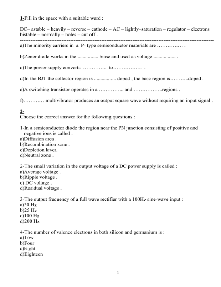
1-Fill in the space with a suitable ward : DC– astable – heavily – reverse – cathode – AC – lightly–saturation – regulator – electrons bistable – normally – holes – cut off . ---------------------------------------------------------------------------------------------------------------a)The minority carriers in a P- type semiconductor materials are …………… . b)Zener diode works in the ................ biase and used as voltage ................. . c)The power supply converts ………….. to…………….. . d)In the BJT the collector region is ................. doped , the base region is………..doped . e)A switching transistor operates in a …………... and ……………..regions . f)………… multivibrator produces an output square wave without requiring an input signal . 2Choose the correct answer for the following questions : 1-In a semiconductor diode the region near the PN junction consisting of positive and negative ions is called : a)Diffusion area . b)Recombination zone . c)Depletion layer. d)Neutral zone . 2-The small variation in the output voltage of a DC power supply is called : a)Average voltage . b)Ripple voltage . c) DC voltage . d)Residual voltage . 3-The output frequency of a full wave rectifier with a 100HZ sine-wave input : a)50 HZ b)25 HZ c)100 HZ d)200 HZ 4-The number of valence electrons in both silicon and germanium is : a)Tow b)Four c)Eight d)Eighteen 1 5-The average value of the 200V peak applied to the half wave rectifier is : a)54.9V b)70.6V c)31.8V d)63.6V 6-A diode clipping circuit : a)Insertes a dc level b)Increases the peak value of the input c)Removes a part of waveform d)Gives average value 7-For normal operation of a NPN transistor the base must be : a)Negative with respect to emitter b)Positive with respect to collector c)0V d)Positive with respect to emitter 8-When a transistor is in a cut-off VCE is equal to : a)0V. b)Vcc . c)0.7V. d)0.1V. 9-If the DC is 0.99 the DC is : a)99 . b)120 . c)100 . d)0.01. 10-The N-type in a PNP transistor is : a)Emitter. b)Base and collector . c)Emitter and collector. d)Base. 2 31- For the circuit shown find : (2 marks) Si a) Diode current (Id) . b) Load voltage (VL) . Ge + Vdc= 17.4V - RL b)For the shown circuit draw the output waveform and plot the voltages on it . (2.5 marks) R Vo V0 +10v 3V Vi t -10v c)Write the name and function for the following symbols : (3 marks) symbol name function 1- .......................... ............................. 2- ........................... .............................. 3- ............................ .............................. 3 4The figure shown below is the main stages of DC power supply . 1 2 3 Vi 3 44 IL + VL RL - Write these main stages and its function with output waveforms by using the table below : Stage Name Output waveform 1 2 3 4 4 Function 55 : 1 For the shown circuit : Vi = 110 Vrms a)What type of this circuit ? ..............................................................F= 50 HZ RL = 1K b)What is the peak primary voltage (VPRI) ? ........................................................................ ........................................................................ c)What is the peak secondary voltage (VPS) ? ........................................................................ ........................................................................ d)What is the peak output voltage (VPO) ? ........................................................................ ......................................................................... e)Sketch the output waveform . f) What is the average output voltage (VOavg) ? ........................................................................ ......................................................................... g) What is the peak output current (IPO) ? ........................................................................ ......................................................................... h)If a capacitance filter 100 F is connected in parallel with the load calculate : r % = ............................................................ ............................................................ 5 6a)For the shown circuit : VS= 24 V VL= 15 V R=0.5K 1)Find the value of IL , IT , IZ 2)The power dissipated in the resistance (PR) . (3marks) RL=1.5K R + Vs=24V IT IL VZ - b)A transistor has collector current 3ma and DC of 0.97 find base current . (2marks) c) A transistor has base current 0.2 ma and emitter current 8 ma find its DC and DC . (3marks) 6 RL 7For the shown circuit : (βDC=100) Calculate IB , IC , IE , VRC ,VCE . Vcc =+20V RC VBB = 4.7V 7 RB 4 8a-Determine which of the following diodes are conducting(forward) and which are nonconducting(reverse) ? find also V0 . (3 marks) +3V +2V VO +1V R b) 2)For the shown circuits : a)Construct voltage and logic truth table . b)Determine the logic operation performed . (6 marks) +5V R2 A V0 B R1 0V +5V +5V A B F outpu 8 9For the shown circuit : VCC RC1 F R1 RC2 R2 47 C1 Q1 Q2 D INPUT= 2 KHZ C R a)What type of this circuit . ................................................................... b)Draw the waveform of the input and output . c)Calculate the pulse width (pw) . ................................................................... ................................................................... .................................................................. d) Calculate the time period (T) . ................................................................... ................................................................... .................................................................... e) Calculate the frequency of the output (F) . ................................................................... ................................................................... .................................................................. f) Calculate the duty cycle of the output . ................................................................... ................................................................... 9
