supporting information
advertisement
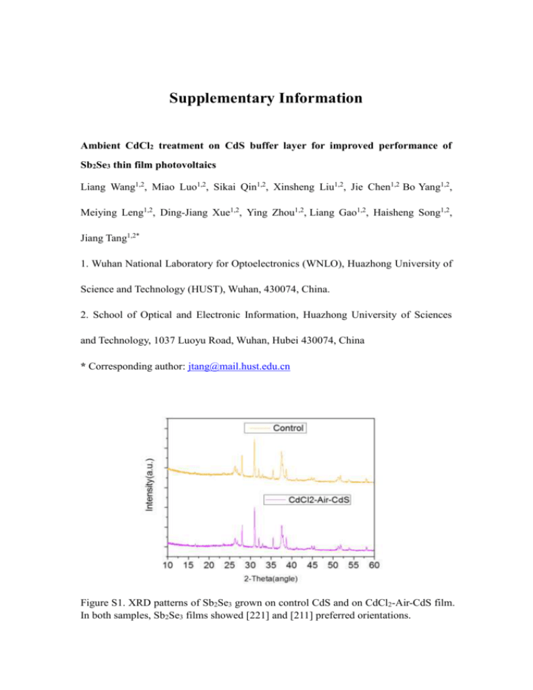
Supplementary Information Ambient CdCl2 treatment on CdS buffer layer for improved performance of Sb2Se3 thin film photovoltaics Liang Wang1,2, Miao Luo1,2, Sikai Qin1,2, Xinsheng Liu1,2, Jie Chen1,2 Bo Yang1,2, Meiying Leng1,2, Ding-Jiang Xue1,2, Ying Zhou1,2, Liang Gao1,2, Haisheng Song1,2, Jiang Tang1,2* 1. Wuhan National Laboratory for Optoelectronics (WNLO), Huazhong University of Science and Technology (HUST), Wuhan, 430074, China. 2. School of Optical and Electronic Information, Huazhong University of Sciences and Technology, 1037 Luoyu Road, Wuhan, Hubei 430074, China * Corresponding author: jtang@mail.hust.edu.cn Figure S1. XRD patterns of Sb2Se3 grown on control CdS and on CdCl2-Air-CdS film. In both samples, Sb2Se3 films showed [221] and [211] preferred orientations. Figure S2. PL spectra of CdS with different treatment: Control, N2-CdS, Air-CdS, CdCl2-Air-CdS. Obviously, thermal annealing (N2-CdS) has negligible effect on CdS photoluminescence, and oxygen has a strong positive effect on CdS defects passivation, as evidenced by the significant enhancement of band edge emission (~2.25 eV peak) and strong suppression of the defect emission (~1.75 eV) in the Air-CdS sample.
