File
advertisement
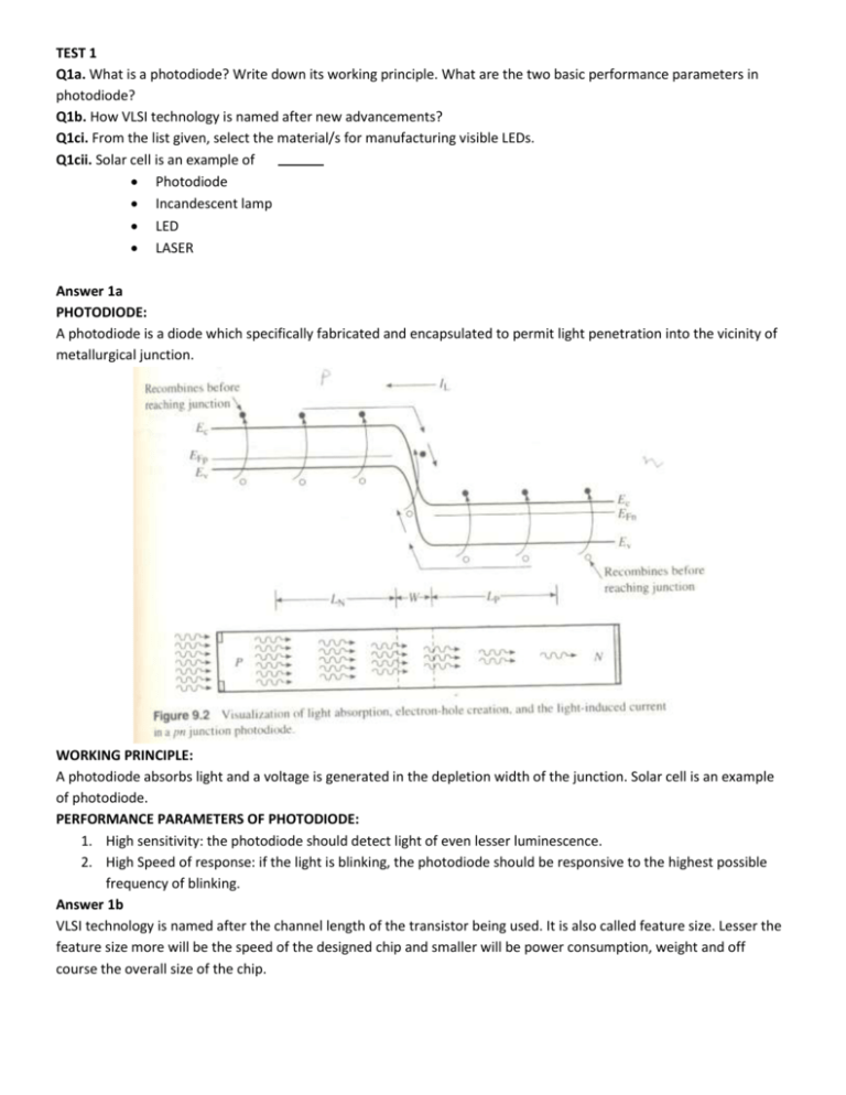
TEST 1 Q1a. What is a photodiode? Write down its working principle. What are the two basic performance parameters in photodiode? Q1b. How VLSI technology is named after new advancements? Q1ci. From the list given, select the material/s for manufacturing visible LEDs. Q1cii. Solar cell is an example of Photodiode Incandescent lamp LED LASER Answer 1a PHOTODIODE: A photodiode is a diode which specifically fabricated and encapsulated to permit light penetration into the vicinity of metallurgical junction. WORKING PRINCIPLE: A photodiode absorbs light and a voltage is generated in the depletion width of the junction. Solar cell is an example of photodiode. PERFORMANCE PARAMETERS OF PHOTODIODE: 1. High sensitivity: the photodiode should detect light of even lesser luminescence. 2. High Speed of response: if the light is blinking, the photodiode should be responsive to the highest possible frequency of blinking. Answer 1b VLSI technology is named after the channel length of the transistor being used. It is also called feature size. Lesser the feature size more will be the speed of the designed chip and smaller will be power consumption, weight and off course the overall size of the chip. The distance between source and drain is channel length, that is also called feature size and technology is named after this feature size. L= channel length Answer 1ci For visible LEDs, two requirements must be fulfilled 1. The material should be a direct band gap semiconductor 2. The band gap energy of semiconductor must fall in between the visible range, i.e. 1.7< Eg < 3.1 (eV) Answer 1cii Solar cell is an example of photodiode. TEST 2 Q2a. What different kinds of processes are used for thin film deposition? Explain each briefly. Q2b. What are the characteristics of GaAs0.6P0.4 LED? Explain with the help of diagram. Q2ci. From the list given, select the material/s for manufacturing infrared LEDs. Q2cii. The creation of voltage (or current) in a material due to exposure to electromagnetic radiation is Photoelectric effect Photovoltaic effect Hall Effect All of the above Answer 2a THIN FILM DEPOSITION: thin films are deposited over a chip in order to form required connections and materials to produce a finished device. Usually interconnections and electrical isolation are made by thin film depositions. The following processes are used for thin film deposition. Evaporation: The source material to be deposited is placed in or on a resistance heated source holder inside a vacuum chamber. To evaporate Al, for example, a short piece of Al wire would be place on a tungsten filament or boat. The substrate, on which the Al is to be deposited over, is also place inside the chamber facing the source. The chamber is then evacuated, power supplied to the holder and The source vaporized. Sputtering: In sputtering the source material and the substrate (wafer) are placed on opposing parallel plates connected to a high voltage power supply. The chamber is evacuated to air and then Argon (Ar) is admitted into the chamber. Applying an interelectrode voltage ionizes the Ar gas and creates a plasma between the plates. The source material is made as cathode, and Ar+ ions move towards the cathode and causesource atoms/molecules to be ejected. The ejected particles move towards substrate where they deposit to form desired thin film. Fig. sputtering Chemical vapor deposition: In CVD the thin film is formed from one or more gas phase components. Either a compound decomposes to form the film or reaction between gas components takes place to form the film. The CVD reactions are surface catalyzed, preferentially taking place on the surface of wafers inserted into the gas stream. Types of CVD are Atmospheric pressure chemical vapor deposition (APCVD or CVD) Low pressure chemical vapor deposition (LPCVD) Plasma enhanced chemical vapor deposition (PECVD) Answer 2b THE CHARACTERISTICS of GaAs0.6P0.4 LED The combination of GaAs and GaP forms a compound GaAs1-xPx Changing the composition of As and P changes the characteristics. The variable x helps in calculation of composition quantity. Value of x=0.4 is specifically used for making optimized LED performance. Regarding direct bandgap and light output efficiency. STRUCTURE The substrate is made of n type GaAs. The next layer is graded in composition by changing the value of x, gradually from 0 to 0.4. these grades are required for lattice matching of GaAs and GaAs1-xPx otherwise there will be defects of lattice mismatch if we form a layer of GaAs0.6P0.4 directly over GaAs. The increased x produces wider Eg. Finally Zn is diffused into the upper layers to form p side of the junction. Answer 2ci For manufacturing infrared LEDs the material must have direct bandgap and the Eg should be less than 1.7eV. Since from the given list of materials, GaAs has Eg of 1.43 it is suitable for manufacturing of infrared LEDs. Answer 2cii The creation of voltage (or current) in a material due to exposure to electromagnetic radiation is Photovoltaic effect TEST 3 Q3a. In optics what are the three causes of excitation of electrons from valence to conduction band? Explain briefly. Q3b. What do you mean by wafer in electronic materials? Write down the steps how do we obtain a wafer; starting from electronic grade silicon. Q3ci. From the list given, select the material/s for manufacturing ultraviolet LEDs. Q3cii. The Electromagnetic radiations when fall on a semiconductor gets absorbed if λ of incident ray is than/to λ of the exposed material. Greater Equal Smaller In comparable Answer 3a The general property of light emission is called Luminescence. This can be divided according to the excitation mechanism. The electrons can be excited in three ways. PHOTOLUMINESCENCE: If carriers are excited by photon absorption, the radiation resulting from the recombination of the excited carriers is called photoluminescence. CATHODOLUMINESCENCE: If the excited carriers are created by high energy electron bombardment of the material, the mechanism is called cathodoluminescence. ELECTROLUMINESCENCE: If the excitation occurs by the introduction of current into the sample, the resulting luminescence is called electroluminescence. Answer 3b WAFER The ultrapure silicon ingot (in cylindrical shape) is cut into discs of at most 1mm thickness. These slices are called wafers. A wafer is base material for the manufacturing process of semiconductor devices. Czochralski method is used to obtain wafer out of polycrystalline Si. The steps are as follows. 1. Ultrapure polycrystalline Si is placed in quartz crucible and heated in inert atmosphere. 2. A small single crystal or Si seed with normal to its bottom face, carefully aligned along a predetermined direction, is clamped to a metal rod and dipped into the metal. 3. Gradually rotate and pull out to maintain thermal equilibrium throughout the crystal. 4. Finally a cylindrical shaped ingot is formed which is 1 to meters long and usually have a diameter of around 8 inches. 5. It is then cut into slices of around 1mm thickness through a diamond edge saw. These slices are called wafers! Answer 3ci Aluminium Nitride (AlN) is the material from the given list that is suitable for manufacturing UV LEDs since its Eg=6.2eV and it is directband gap. This shows that radiation of wavelength of less than 0.2um can get absorbed into it and UV radiations have wavelength of less than 0.4 um. Answer 3cii The Electromagnetic radiations when fall on a semiconductor gets absorbed if λ of incident ray is smaller than/to λ of the exposed material. TEST 4 Q4a. Differentiate between photoelectric and photovoltaic effect. Q4b. What do you know about lithography? Explain with the help of diagram. Q4ci. From the list given, select the material/s for manufacturing blue LEDs. Q4cii. In LEDs and LASERs, generally semi conductors are used Indirect band gap Degenerate Non-degenerate Direct band gap Answer 4a PHOTOELECTRIC EFFECT is phenomenon in which electrons are emitted from matter as a consequence of their absorption of energy from electromagnetic radiations. (kindly label the diagram yourself) PHOTOVOLTAIC EFFECT involves creation of voltage (or current) in a material upon exposure to electromagnetic radiations. An illustration of solar cell depicting photovoltaic effect Answer 4b PHOTOLITHOGRAPHY: Photolithography (or "optical lithography") is a process used in micro-fabrication to selectively remove parts of a thin film or the bulk of a substrate. It uses light to transfer a geometric pattern from a photo mask to a light-sensitive chemical photo resist, or simply "resist," on the substrate. A series of chemical treatments then engraves the exposure pattern into the material underneath the photo resist. (you can draw any one of the following diagrams) Answer 4ci For manufacturing blue LED, the material must be direct bandgap and its Eg should correspond to the wavelength of blue light. ZnSe and GaN fulfills the above criteria. Answer 4cii In LEDs and LASERs, generally direct band gap semi conductors are used. TEST 5 Q5a. Why can’t GaAs and GaP be used in forming visible LEDs? Which alloy is used for that? Q5b. What do you know about chemical vapor deposition? Q5ci. Can you use Si for making LASERs? Justify your answer. Q5cii. Band gap is difference between Conduction band and valence bands Majority and minority carriers Direct and indirect bands Degenerate and non degenerate Answer 5a GaAs is a direct semiconductor, but its band gap is too small to produce visible light emission. GaP has a λG in the visible range but is indirect. Individually neither compound meets the LED material requirements. However, a combination of these two compounds the GaAs1-x Px alloy is both direct and has a light-producing EG for x values in the range 0.28 ≤ x ≤ 0.45. GaAs0.6 P0.4 with an x=0.4 is specifically used as the light emitting material because it yields an output that appears brightest to the human eye. As x is increased, the output wavelength decreases and the human eye response increase by a factor of ~50. The product of LED efficiency and the eye response exhibits a maximum at x=0.4. This value is used in producing commercial devices. Answer5b CHEMICAL VAPOR DEPOSITION: Any CMOS process requires the repetitive deposition of layers of a material over the complete wafer, to either act as buffers for a processing effect, or as insulating or conducting layers. In CVD the thin film is formed from one or more gas phase components, with energy supplied by heat. Either a compound decomposes to form the film or reaction between gas components takes place to form the film. The CVD reactions are surface catalyzed, preferentially taking place on the surface of wafers inserted into the gas stream. Types of CVD are Atmospheric pressure chemical vapor deposition (APCVD or CVD) Low pressure chemical vapor deposition (LPCVD) Plasma enhanced chemical vapor deposition (PECVD) Answer5ci No, silicon cannot be used for manufacturing of LEDs, since it is indirect band gap. Although Si compounds can be used like SiC and SiGe. Answer5cii Band gap is difference between conduction band and valence bands TEST 6 Q6a. Differentiate between PIN and avalanche photodiode. Q6b. How do we get electronic silicon grade out of soil? Explain with the help of block diagram. Q6ci. Can visible spectrum of electromagnetic radiations gets absorbed into diamond? Justify your answer. Q6cii. LASER action occurs due to of radiation Spontaneous emission Stimulated emission Absorption Interference Answer 6a DIFFERENCE BETWEEN PIN AND AVALANCHE PHOTODIODE PIN is a three region structure in which intrinsic region is sandwiched between heavily doped p and n regions. P+ region is made very thin to minimize absorption. The thickness of i-layer is tailored according to the requirements of sensitivity and speed of response. Since the photons get absorbed within depletion region therefore width of depletion region must be large and in PIN intrinsic layer serves the purpose. When photons get absorbed, electron hole pairs are produced and then they drift towards their respective sides, therefore width should not be so large too. ADVANTAGES OF PIN: 1. The diode can be optimized for response at a given λ by making intrinsic width equal to inverse of absorption coefficient (1/ Answer 6b The readily available soil (silica) after going through numerous process transforms into electronic grade silicon, to be used for manufacturing of Integrated circuits (ICs). The steps are as under: Silica is heated with carbon in an electric furnace to produce low grade silicon or ferrosilicon. The carbon pulls oxygen away from the impure SiO2. Next, ferrosilicon is chlorinated to yield SiCl4 or SiHCl3, both are liquids at room temperature. After multiple distillations and liquid purification procedures an ultrapure SiCl4 or SiHCl3 is obtained. Lastly, the high purity halide is chemically reduced, yielding the desired ultrapure elemental silicon. TEST 7 Q7a. What is the difference between direct and indirect bandgap semiconductors? Answer 6ci Answer 6cii Answer 6ci No, EMR of visible spectrum do not get absorbed into diamond since the band gap is 5.46eV which is so large as compared to the complete range of visible spectrum (from 1.7eV to 3.1eV). Answer 6cii LASER action occurs due to stimulated emission of radiation. TEST 7 Q7a. What is the difference between direct and indirect band gap semiconductors? Q7b. What are the three categories of solar cells? Name them and write briefly about them. Application and distinguishing feature Q7ci. Can you use Ge for making LASERs? Justify your answer. Q7cii. Thin film can be dopsited by process of Ion implantation Photolithography Chemical vapor deposition Doping Answer 7a Answer 7b Answer 7ci No, germanium cannot be used for manufacturing of LEDs, since it is indirect band gap. Answer 7cii Thin film can be dopsited by process of Chemical vapor deposition TEST 8 Q8a. What is the difference between spontaneous and stimulated emission of radiation? Q8b. A particular material becomes transparent for a specific range of optical wavelengths and opaqe for the rest of the wavelengths, what is its reason? Q8ci. From the list given, select the material/s for manufacturing blue LEDs. Q8cii. The VLSI technology is recognized by of CMOS process Cost Speed Power consumption Feature size Answer 8a Answer 8b Answer 8ci Answer 8cii TEST 9 Q9a. What are the two requirements for high stimulation emission in LASERs? Q9b. How do you describe dual nature of electron? What information can be obtained by Schrodinger equation? Q9ci. If violet light falls on SiC will it get absorbed or SiC remains transparent? Q9cii. In GaAs, if Ga atoms are replaced by Si atoms then it will become n-type p-type Compensated semiconductor Doped semiconductor TEST 10 Q10a. What is the difference in working principle of LED and LASER? Q10b. How materials are classified in composition and in structure? Q10ci. If a light of wavelength 0.688um strikes AlAs, will it be opaque or transparent? Justify your answer. Q10cii. When NA and ND are comparable and non-zero, the material is said to be semiconductor. Doped compensated intrinsic extrinsic
