Electricity Questions: Electrons at work
advertisement
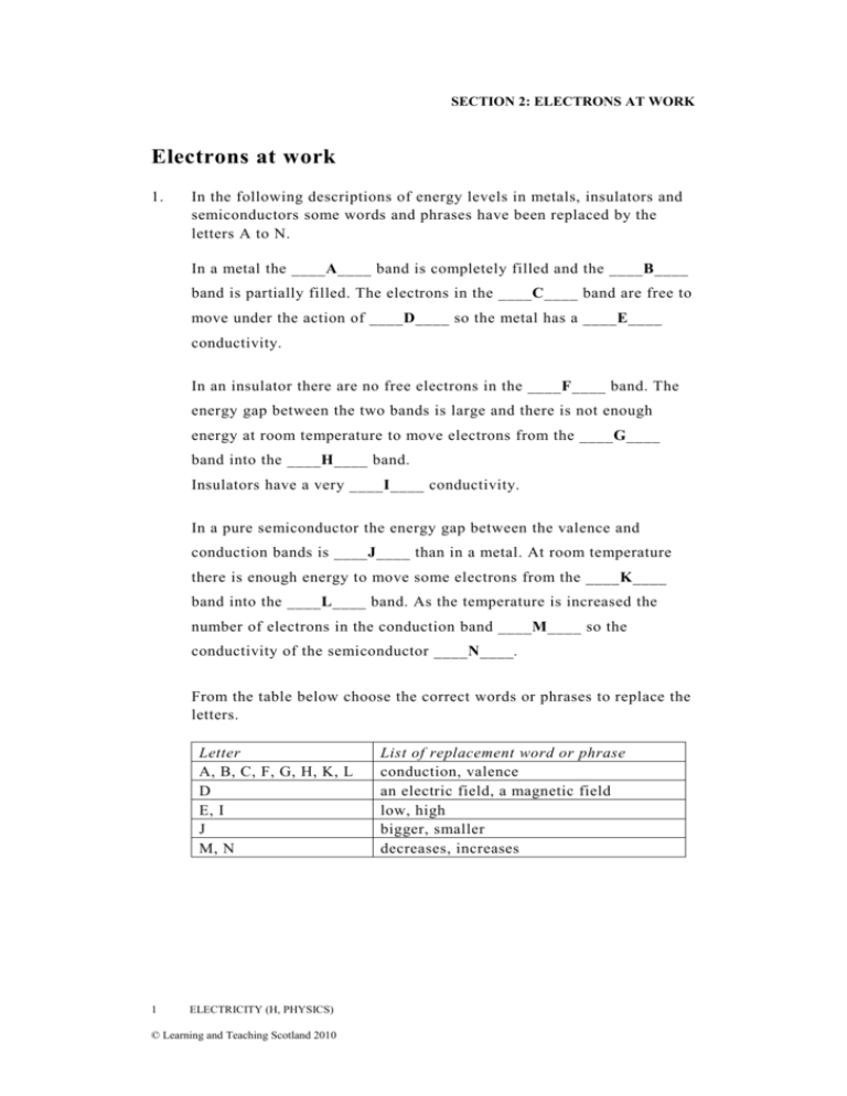
SECTION 2: ELECTRONS AT WORK Electrons at work 1. In the following descriptions of energy levels in metals, insulators and semiconductors some words and phrases have been replaced by the letters A to N. In a metal the ____A____ band is completely filled and the ____B____ band is partially filled. The electrons in the ____C____ band are free to move under the action of ____D____ so the metal has a ____E____ conductivity. In an insulator there are no free electrons in the ____F____ band. The energy gap between the two bands is large and there is not enough energy at room temperature to move electrons from the ____G____ band into the ____H____ band. Insulators have a very ____I____ conductivity. In a pure semiconductor the energy gap between the valence and conduction bands is ____J____ than in a metal. At room temperature there is enough energy to move some electrons from the ____K____ band into the ____L____ band. As the temperature is increased the number of electrons in the conduction band ____M____ so the conductivity of the semiconductor ____N____. From the table below choose the correct words or phrases to replace the letters. Letter A, B, C, F, G, H, K, L D E, I J M, N 1 ELECTRICITY (H, PHYSICS) © Learning and Teaching Scotland 2010 List of replacement word or phrase conduction, valence an electric field, a magnetic field low, high bigger, smaller decreases, increases SECTION 2: ELECTRONS AT WORK 2. The conductivity of a semiconductor material can be increased by ‘doping’. (a) (b) (c) 3. (a) (b) 4. an n-type semiconductor material a p-type semiconductor material. A p-n junction diode is connected across a d.c. supply as shown. (a) (b) (c) 6. A sample of pure germanium (four electrons in the outer shell) is doped with phosphorus (five electrons in the outer shell). What kind of semiconductor is formed? Why does a sample of n-type semiconductor still have a neutral overall charge? Describe the movement of the majority charge carriers when a current flows in: (a) (b) 5. Explain what is meant by the ‘conductivity’ of a material. Explain, giving an example, what is meant by ‘doping’ a semiconductor. Why does ‘doping’ decrease the resistance of a semiconductor material? Is the diode connected in forward or reverse bias mode? Describe the movement of the majority charge carriers across the p-n junction. What kind of charge is the only one that actually moves across the junction? When positive and negative charge carriers recombine at the junction of ordinary diodes and LEDs, quanta of radiation are emitted from the junction. (a) (b) Does the junction have to be forward biased or reverse biased for radiation to be emitted? What form does this emitted energy take when emitted by: (i) an LED (ii) an ordinary junction diode? SECTION 2: ELECTRONS AT WORK 7. 8. A particular LED is measured as having a recombination energy of 3·12 × 10 –19 J. (a) (b) (c) Calculate the wavelength of the light emitted by the LED. What colour of light is emitted by the LED? What factor about the construction of the LED determines the colour of the emitted light? (a) State two advantages of an LED over an ordinary filament lamp. (b) An LED is rated as follows: operating p.d. 1·8 V, forward current 20 mA The LED is to be operated from a 6 V d.c. power supply. (i) (ii) 9. The diagram shows a photodiode connected to a voltmeter. (a) (b) 3 Draw a diagram of the circuit, including a protective resistor, which allows the LED to operate at its rated voltage. Calculate the resistance of the protective resistor that allows the LED to operate at its rated voltage. In which mode is the photodiode operating? Light is now incident on the photodiode. (i) Explain how an e.m.f. is created across the photodiode. (ii) The irradiance of the light incident on the photodiode is now increased. Explain why this increases the e.m.f. of the photodiode. ELECTRICITY (H, PHYSICS) © Learning and Teaching Scotland 2010 SECTION 2: ELECTRONS AT WORK 10. A photodiode is connected in reverse bias in a series circuit as shown. (a) (b) (c) (d) In which mode is the photodiode is operating? Why is the photodiode connected in reverse bias? What is the current in the circuit when the photodiode is in darkness? Explain your answer. The irradiance of the light on the photodiode is now increased. (i) What is the effect on the current in the circuit? (ii) What happens to the effective ‘resistance’ of the photodiode? Explain why this happens. SOLUTIONS Solutions Electrons at work 1. A = valence; B = conduction; C = conduction; D = an electric field; E = high; F = conduction; G = valence; H = conduction; I = low; J = smaller; K = valence; L = conduction; M = increases; N = increases. 7. (a) (b) 638 nm Red 8. (b) (ii) 5 ELECTRICITY (H, PHYSICS) 210 Ω © Learning and Teaching Scotland 2010
![Semiconductor Theory and LEDs []](http://s2.studylib.net/store/data/005344282_1-002e940341a06a118163153cc1e4e06f-300x300.png)
