final 2015
advertisement
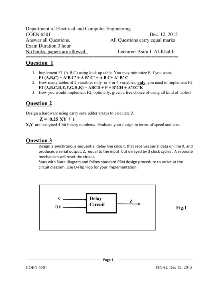
Department of Electrical and Computer Engineering COEN 6501 Dec. 12, 2015 Answer all Questions. All Questions carry equal marks Exam Duration 3 hour No books, papers are allowed. Lecturer: Asim J. Al-Khalili =============================================================== Question 1 1. Implement F1 (A,B,C) using look up table. You may minimize F if you want. F1 (A,B,C) = A’B C’ + A B’ C’ + A B C+ A’ B’ C 2. How many tables of 2 variables only or 3 or 4 variables, only, you need to implement F2 F2 (A,B.C,D,E,F,G,H,K) = ABCD + F + B’GH + A’EC’K 3. How you would implement F2, optimally, given a free choice of using all kind of tables? Question 2 Design a hardware using carry save adder arrays to calculate Z. Z = 0.25 XY + 1 X,Y are unsigned 4-bit binary numbers. Evaluate your design in terms of speed and area Question 3 Design a synchronous sequential delay line circuit, that receives serial data on line X, and produces a serial output, Z, equal to the input but delayed by 3 clock cycles . A separate mechanism will reset the circuit. Start with State diagram and follow standard FSM design procedure to arrive at the circuit diagram. Use D-Flip Flop for your implementation. X CLK Delay Circuit Z Fig.1 Page 1 COEN 6501 FINAL Dec 12. 2015 Question 4 a. Identify all the paths in the circuit shown in the Fig. 2 below. b. Determine maximum speed of operation at typical conditions. Timing parameters for all components are listed in Table 1. c. At the maximum speed of operation, determine the slack time for the setup time and hold time at the K-input of Flip-Flop U5. Is there any violation? Fig. 2 Component Tp (ns) Input Loading (UL) K1 K2 ns/fanout ns/UL Inverter 0.1 1 0.1 0.08 XOR(2input) 0.20 2 0.05 0.14 AND (2 input) 0.4 1.5 0.12 0.18 Flip Flop, ↑, (CK to Q) 1.5 2 0.15 0.2 Tsu=1 ns, th = 0.5ns Table 1 Page 2 COEN 6501 FINAL Dec 12. 2015 Question 5 a. The Circuit shown in Fig. 2 operates at a frequency 50 MHz. Signal A and B arrive at -∞. Determine the arrival time, the required time and the slack time at points F. b. Determine the maximum clock frequency, considering worst case scenario. The circuit is implemented on a die, packaged in a ceramic DIP with a thermal resistance of 30oC/W. Power consumption of the chip is 1.5 W with room temp at 25 oC. Fanout loading is neglected. Voltage variation can be ± %5. Use Table 2 parameters. Fig. 2 (Tp K1 Ni K 2 ML) * K ' , TJ = Tamb + Φ Ja * Pd KV = Tj KT = Ta K’ = KT * KV *K p 1 1 0.01 * fV , 1 .5 KP = 1+ 0.01 * fP Component Tp (ns) Input Loading (UL) AND/(2input) 0.2 1 0.15 INV 0.1 2 0.25 XOR (3 input) 0.4 3 0.35 Flip Flop, ↑, (CLK to Q) 2 4 0.45 K1 ns/UL Tsu=1 ns, th = 0.5ns , tskew=2ns Table 2 Page 3 COEN 6501 FINAL Dec 12. 2015 Question 6 Design a bit comparator shown in Fig 3, then using iterative method design an 8-bit comparator shown in Fig. 4. Using VHDL, and the bit comparator as a component, write the code for an 8-bit comparator. Fig. 3 Fig. 4 ===================================================================== Appendix A 1. tcs,max < tCQmin + tCLmin + tsu.min 2. Tmin tCQmax + tCLmax+ tsUmaxR2 –tcsmin 3. thmaxR2 < tCQmin + tCLmin - tcsmax Page 4 COEN 6501 FINAL Dec 12. 2015 tCL = tLogic + tinterconnec Page 5 COEN 6501 FINAL Dec 12. 2015
