Midterm study guide
advertisement
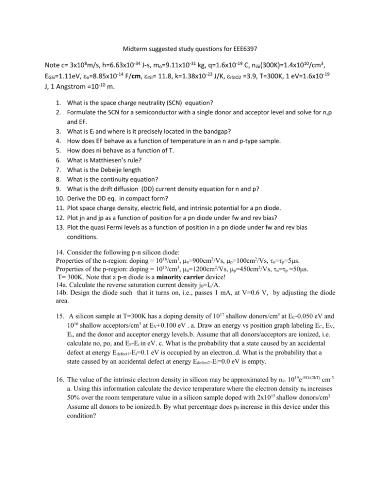
Midterm suggested study questions for EEE6397 Note c= 3x10⁸m/s, h=6.63x10⁻³⁴ J-s, mo=9.11x10⁻³¹ kg, q=1.6x10⁻¹⁹ C, niSi(300K)=1.4x10¹⁰/cm3, EGSi=1.11eV, o=8.85x10⁻¹⁴ F/cm, rSI= 11.8, k=1.38x10⁻²³ J/K, rSIO2 =3.9, T=300K, 1 eV=1.6x10⁻¹⁹ J, 1 Angstrom =10-10 m. 1. What is the space charge neutrality (SCN) equation? 2. Formulate the SCN for a semiconductor with a single donor and acceptor level and solve for n,p and EF. 3. What is Ei and where is it precisely located in the bandgap? 4. How does EF behave as a function of temperature in an n and p-type sample. 5. How does ni behave as a function of T. 6. What is Matthiesen’s rule? 7. What is the Debeije length 8. What is the continuity equation? 9. What is the drift diffusion (DD) current density equation for n and p? 10. Derive the DD eq. in compact form? 11. Plot space charge density, electric field, and intrinsic potential for a pn diode. 12. Plot jn and jp as a function of position for a pn diode under fw and rev bias? 13. Plot the quasi Fermi levels as a function of position in a pn diode under fw and rev bias conditions. 14. Consider the following p-n silicon diode: Properties of the n-region: doping = 1016/cm3, n=900cm2/Vs, p=100cm2/Vs, n=p=5s. Properties of the p-region: doping = 1015/cm3, n=1200cm2/Vs, p=450cm2/Vs, n=p =50s. T= 300K. Note that a p-n diode is a minority carrier device! 14a. Calculate the reverse saturation current density j0=Io/A. 14b. Design the diode such that it turns on, i.e., passes 1 mA, at V=0.6 V, by adjusting the diode area. 15. A silicon sample at T=300K has a doping density of 1017 shallow donors/cm3 at EC-0.050 eV and 1016 shallow acceptors/cm3 at EV+0.100 eV . a. Draw an energy vs position graph labeling EC, EV, Ei, and the donor and acceptor energy levels.b. Assume that all donors/acceptors are ionized, i.e. calculate no, po, and EF-Ei in eV. c. What is the probability that a state caused by an accidental defect at energy Edefect1-Ei=0.1 eV is occupied by an electron..d. What is the probability that a state caused by an accidental defect at energy Edefect2-Ei=0.0 eV is empty. 16. The value of the intrinsic electron density in silicon may be approximated by ni= 1019e-EG/(2kT) cm-3. a. Using this information calculate the device temperature where the electron density n0 increases 50% over the room temperature value in a silicon sample doped with 2x10¹⁵ shallow donors/cm3. Assume all donors to be ionized.b. By what percentage does p0 increase in this device under this condition?
