CST workflow
advertisement
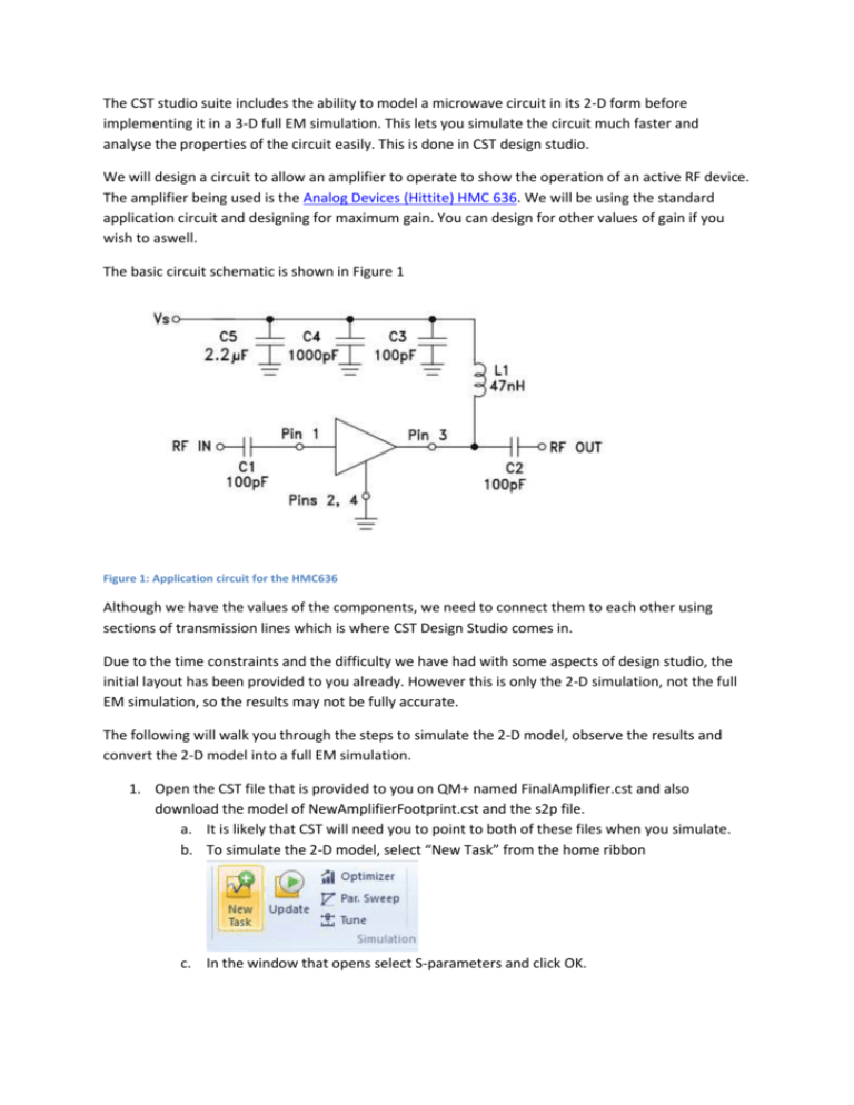
The CST studio suite includes the ability to model a microwave circuit in its 2-D form before implementing it in a 3-D full EM simulation. This lets you simulate the circuit much faster and analyse the properties of the circuit easily. This is done in CST design studio. We will design a circuit to allow an amplifier to operate to show the operation of an active RF device. The amplifier being used is the Analog Devices (Hittite) HMC 636. We will be using the standard application circuit and designing for maximum gain. You can design for other values of gain if you wish to aswell. The basic circuit schematic is shown in Figure 1 Figure 1: Application circuit for the HMC636 Although we have the values of the components, we need to connect them to each other using sections of transmission lines which is where CST Design Studio comes in. Due to the time constraints and the difficulty we have had with some aspects of design studio, the initial layout has been provided to you already. However this is only the 2-D simulation, not the full EM simulation, so the results may not be fully accurate. The following will walk you through the steps to simulate the 2-D model, observe the results and convert the 2-D model into a full EM simulation. 1. Open the CST file that is provided to you on QM+ named FinalAmplifier.cst and also download the model of NewAmplifierFootprint.cst and the s2p file. a. It is likely that CST will need you to point to both of these files when you simulate. b. To simulate the 2-D model, select “New Task” from the home ribbon c. In the window that opens select S-parameters and click OK. d. Ensure the tick box for Maximum Frequency Range is selected and then click Ok on this box too. e. Now click on Update (play button) – let it simulate. Any errors that occur try to fix them yourself before asking… f. In the navigation tree on the left hand side (bottom left) you will find your results g. From here, you can take a look at your results and check that you are getting good Sparameter results. 2. Next we have to check the layout is correct. a. Click on the layout button from the home ribbon b. In the new window which appears click on ‘snap all components’ c. Allow it to work through the processes and the design should come out exactly as shown below in Figure 2 Figure 2: 3-D Layout of the amplifier 3. If the design looks good, the next step is to simulate it as a full 3-D model. To do this, we must first create a simulation project. a. Return back to the schematic window and click on ‘Simulation Project’ and then click on “all blocks as 3-D model” b. Give the project a name which is different to your amplifier name and fill the boxes out as follows: 4. A 3-D model window will now open which will look familiar as it is CST Microwave Studio. a. Click on setup solver and turn off adaptive mesh refinement, click apply and ok. b. Click on the schematic window next to the 3-D tab at the bottom of the viewing window. c. You should see now that ports 3 and 4 are connected to the touchstone file, ports 1 and 2 are input and output ports and port 5 goes to the DC bias. d. In the schematic view, click on Update again, and now the simulation will run a full 3D EM simulation of the whole structure. e. You can view the simulation results as before. 5. If you make any changes to the design which you would like fabricated, then please email them to p.l.alizadeh@qmul.ac.uk before Wednesday evening.
