in Microsoft Word
advertisement
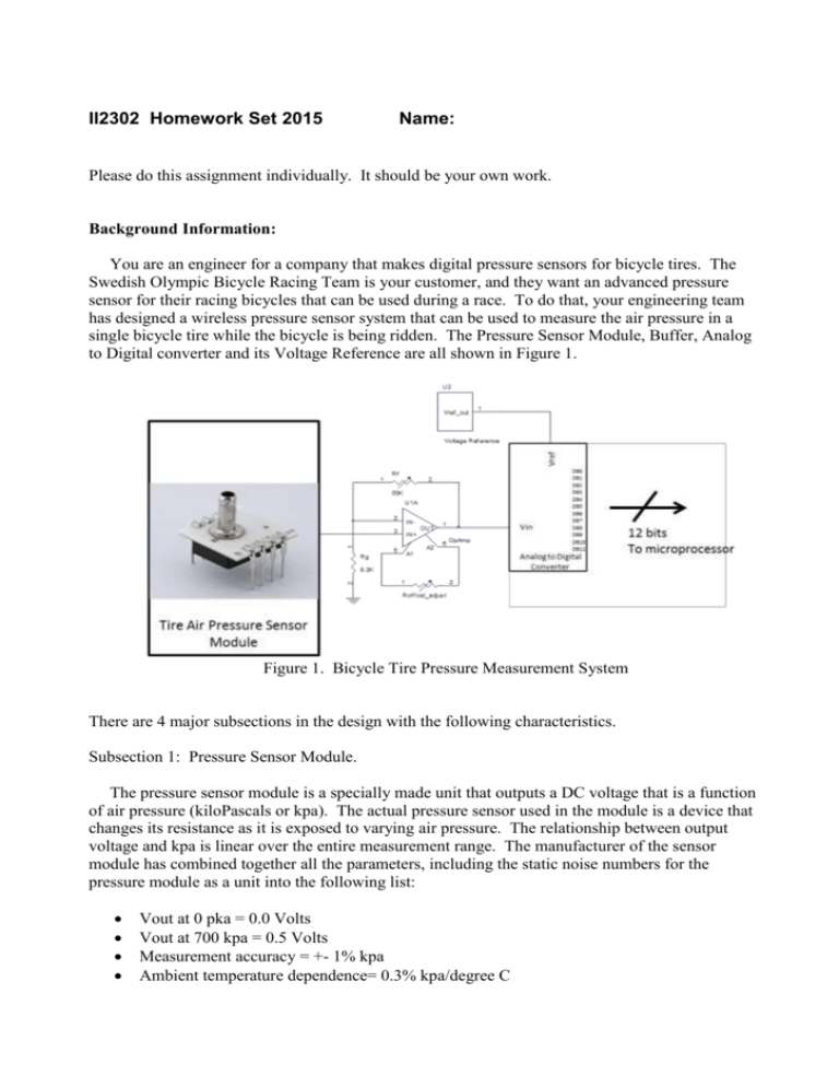
II2302 Homework Set 2015 Name: Please do this assignment individually. It should be your own work. Background Information: You are an engineer for a company that makes digital pressure sensors for bicycle tires. The Swedish Olympic Bicycle Racing Team is your customer, and they want an advanced pressure sensor for their racing bicycles that can be used during a race. To do that, your engineering team has designed a wireless pressure sensor system that can be used to measure the air pressure in a single bicycle tire while the bicycle is being ridden. The Pressure Sensor Module, Buffer, Analog to Digital converter and its Voltage Reference are all shown in Figure 1. Figure 1. Bicycle Tire Pressure Measurement System There are 4 major subsections in the design with the following characteristics. Subsection 1: Pressure Sensor Module. The pressure sensor module is a specially made unit that outputs a DC voltage that is a function of air pressure (kiloPascals or kpa). The actual pressure sensor used in the module is a device that changes its resistance as it is exposed to varying air pressure. The relationship between output voltage and kpa is linear over the entire measurement range. The manufacturer of the sensor module has combined together all the parameters, including the static noise numbers for the pressure module as a unit into the following list: Vout at 0 pka = 0.0 Volts Vout at 700 kpa = 0.5 Volts Measurement accuracy = +- 1% kpa Ambient temperature dependence= 0.3% kpa/degree C The fastest it can respond to changes in pressure over any or all of full range is 1 Hz. Subsection 2: Buffer Stage. The buffer stage is a single operational amplifier opamp circuit with gain and voltage offset adjustments. The gain of the opamp is set to 6 to allow the airflow sensor module to drive the full input range of the analog to digital converter, which is designed to be 0 to 3.0 volts DC. Device characteristics and worst case static noise specifications for the opamp are: Input resistance (Rin) = 1012 ohms Output resistance (Rout) = 100 ohms Input offset voltage temperature drift (TCVos) = 10 uV/degree C Input voltage offset (Vos) = 7mv Input current offset (Ios) = 32pA Voltage noise (Vn) = 37nV over the bandwidth of the device (note, 1nV is 10-9 amps) Hz Current noise (In) = over the bandwidth of the device (note, 1fa is 10-15 amps) 1.5fA Hz Subsection 3: Analog to Digital Converter. The ADC is a 12 bit converter without an internal voltage reference. Input leakage current = 1uA Worst case gain error = 0.5 LSB Worst case input offset error = 0.5 LSB Subsection 4: Voltage Reference. The voltage reference is used to set the voltage input range of the ADC. Output voltage = 3.00 volts Output voltage error = 200 PPM/degree C The specification for the product requires that it measure air pressure over an expected temperature range 0 to 40 degrees C. (Bicycle racers don’t like to race when it is too cold or too hot outside.) Question 1: For all four subsections of the tire air pressure measurement circuit shown in Figure 1, list all of the sources of noise for each subsection and say which noise sources can be calibrated out, and which noise sources must be accounted for as potential output error? Note, we don’t have any other sensors available except those shown in the tire air pressure measurement circuit. Question 2: One of your co-workers on the bicycle tire air pressure product has designed the voltage reference used to set the voltage input range of the ADC. He has told you that he thinks the voltage reference circuit is very low noise which will only result in the loss of 15 LSBs of resolution at most. You have looked at the voltage reference characteristics and you think your coworker is wrong and the actual number of LSBs of resolution lost is much different. What is the actual number of lost LSBs from the noise in the voltage reference? Be sure to show the calculations that give your answer. Question 3: In this question you are working as a consultant at a company that makes sensor based systems. One of your tasks is to evaluate a system that is intended to provide a sensor reading with 7 bits of resolution minimum. The system uses a 10 bit Analog to Digital converter. After you have analyzed the entire system you have found that the total worst case noise for the system is 6 LSBs of resolution. Will this sensor circuit be able to achieve the desired goal of 7 bits of resolution minimum? Show all the calculations you made to get your answer. Question 4: This question has two parts. In this question you are an engineering consultant and your client is a small company that makes sensor based systems. They have hired you to help them solve some serious problems that they have with one of their products. To help with this, you are discussing with them the generalized model of sensor system noise that includes the following parts: One of the parts of the noise model is “Processing” as shown in the picture. Please answer the following two questions. 4A: Explain how processing is a source of noise in sensor based systems. To support your answer give 4 general examples of how processing can result in noise that affects sensor readings. 4B: For each of the 4 examples of how processing can result in noise that affects sensor readings that you listed in problem 4A, suggest a way to minimize the noise. Your suggestions can take advantage of any part of the noise model, but it should be a feasible solution that preserves the system. For example, just saying “do not use a processor” is not very good because it does not preserve the system. Likewise just saying “use a better processor” doesn’t help either because it doesn’t explain what really needs to be made better. Explain your suggestions in enough detail to justify and support what you are trying to say. In other words, explain your suggestions in a way that gives the idea of how and why processor noise can be minimized. Question 5: This problem has 2 parts. In this problem you are working with an engineering team that has designed a sensor for a product that can identify a particular object. To test the system, you have taken measurements using the sensor. First, you have taken repeated measurements of the object the product has been designed to identify. The measurements are plotted in the figure below and are labeled as the “true object”. Next, you have taken repeated measurements of a randomly chosen object that is different from the object the sensor is designed to identify. Those measurements are plotted in the figure below and are labeled “other object”. Note that the X axis is the variance of the data collected expressed in standard deviations. The average for the data labeled “other object” is located at 0 on the X axis. The average for the data labeled “true object” is located at 3 on the X axis. Sensor Data Distributions The data sets clearly overlap. The engineers in your group have decided to design the product in such a way that if the sensor reading is greater than a value on the X axis of 2, then the product will ACCEPT that the object is the “true object”. If the sensor value on the X axis is less than 2 or equal to 2, then the product will REJECT the object as being the “true object”. In this case it will decide that the object is some “other object”. Part 1: For this sensor product, what is the probability of a FALSE ACCEPT when the “other object” is sensed? In other words, what is the probability of an error such that the system will indicate that the object sensed is the “true object” when in reality it is the “other object”? Be sure to show the calculations you used to get your answer. Part 2: For this sensor product, what is the probability of a FALSE REJECT when the “true object” is sensed? In other words, what is the probability of an error such that the system will indicate that the object sensed is the “other object” when in reality it is the “true object”? Be sure to show the calculations you used to get your answer. 20 = 1 21 = 2 22 = 4 23 = 8 24 = 16 25 = 32 26 = 64 27 = 128 28 = 256 29 = 512 210 = 1024 211 = 2048 212 = 4096 Useful Data: chart Useful Data: Powers of 2
