New Standard IGBT Module Technology for Automotive Applications
advertisement
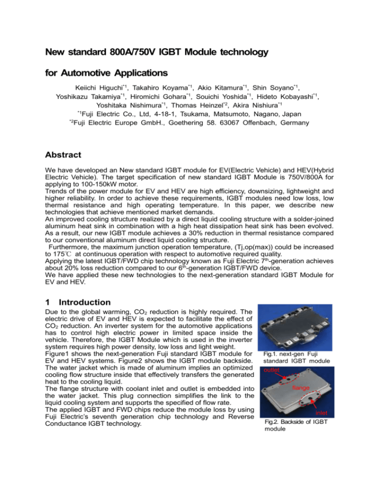
New standard 800A/750V IGBT Module technology for Automotive Applications Keiichi Higuchi*1, Takahiro Koyama*1, Akio Kitamura*1, Shin Soyano*1, Yoshikazu Takamiya*1, Hiromichi Gohara*1, Souichi Yoshida*1, Hideto Kobayashi*1, Yoshitaka Nishimura*1, Thomas Heinzel*2, Akira Nishiura*1 *1 Fuji Electric Co., Ltd, 4-18-1, Tsukama, Matsumoto, Nagano, Japan *2 Fuji Electric Europe GmbH., Goethering 58. 63067 Offenbach, Germany Abstract We have developed an New standard IGBT module for EV(Electric Vehicle) and HEV(Hybrid Electric Vehicle). The target specification of new standard IGBT Module is 750V/800A for applying to 100-150kW motor. Trends of the power module for EV and HEV are high efficiency, downsizing, lightweight and higher reliability. In order to achieve these requirements, IGBT modules need low loss, low thermal resistance and high operating temperature. In this paper, we describe new technologies that achieve mentioned market demands. An improved cooling structure realized by a direct liquid cooling structure with a solder-joined aluminum heat sink in combination with a high heat dissipation heat sink has been evolved. As a result, our new IGBT module achieves a 30% reduction in thermal resistance compared to our conventional aluminum direct liquid cooling structure. Furthermore, the maximum junction operation temperature, (Tj,op(max)) could be increased to 175℃ at continuous operation with respect to automotive required quality. Applying the latest IGBT/FWD chip technology known as Fuji Electric 7th-generation achieves about 20% loss reduction compared to our 6th-generation IGBT/FWD device. We have applied these new technologies to the next-generation standard IGBT Module for EV and HEV. 1 Introduction Due to the global warming, CO2 reduction is highly required. The electric drive of EV and HEV is expected to facilitate the effect of CO2 reduction. An inverter system for the automotive applications has to control high electric power in limited space inside the vehicle. Therefore, the IGBT Module which is used in the inverter system requires high power density, low loss and light weight. Figure1 shows the next-generation Fuji standard IGBT module for EV and HEV systems. Figure2 shows the IGBT module backside. The water jacket which is made of aluminum implies an optimized cooling flow structure inside that effectively transfers the generated heat to the cooling liquid. The flange structure with coolant inlet and outlet is embedded into the water jacket. This plug connection simplifies the link to the liquid cooling system and supports the specified of flow rate. The applied IGBT and FWD chips reduce the module loss by using Fuji Electric’s seventh generation chip technology and Reverse Conductance IGBT technology. Fig.1. next-gen Fuji standard IGBT module outlet flange inlet Fig.2. Backside of IGBT module As result, the module dimension is downsized by new developed IGBT effect. 2 Product information Major features of our new standard IGBT module are listed below: Item Value Collector-Emitter voltage 750V Implemented Collector current 800A Thermal resistance @10l/min 0.13℃/W 175 oC Operating junction temperature Size 162×116×24mm Weight 520g Target motor output power 100-150kW Table 1: Features of next-generation standard IGBT module. These features are achieved by applying the following new technologies. 1. New cooling structure with high cooling performance. 2. Allowing continuous operation at 175°C. 3. Reverse-Conducting IGBT(RC-IGBT) 3 New Cooling Structure with High Cooling Performance 3.1 Subjects for the new cooling structure. The Inverter units, which are used for power control of HEV and EV, are mounted in a limited space. They need to have a compact size and high degree of freedom for mounting, together with weight reduction and efficiency improvement in the view of low fuel consumption. Power modules mounted in inverters also require size and weight reduction as well as efficiency improvement. Size and weight reduction of 20% or more is desired for each upcoming next generation. Especially power modules for automotive applications, in particular, efforts are underway to increase heat radiation to the liquid cooling system. ‘By using an aluminum jacket the weight of the cooling unit can be reduced. Improved heat dissipation performance by designing aluminum cooling fins in direct cooling structure of the IGBT module could be achieved. As a result, Fuji Electric obtained a reduction of the thermal resistance by 30%. This paper describes the design of aluminum cooling structure. 3.2 Technological Issue with Conventional Cooling Structure Figure 3 shows the cross-sectional structure of the conventional Fuji Electric’s IGBT Module with aluminium direct liquid cooling [1]. In this structure, the module and heat sink are directly bonded together by soldering and the water jacket is independently designed. Hence, the heat sink and the water jacket are separated parts. This requires a design process considering water-tightness and tolerance in addition to the flow channel design. For that reason, it is necessary to select materials and choose a base thickness in consideration of buckling and deformation. This was a factor leading to an increase in thermal resistance. In order to solve this issue, ensure the improved heat radiation capacity and high secure the reliability in the aluminium direct liquid cooling structure; Fuji Electric developed an aluminium cooler integrating a heat sink and water jacket. Fig.3. Conventional direct cooling structure. 3.3 Cooler Designing Technology The heat radiation performance of a power module can be represented by two parameters: thermal resistance and thermal conductivity coefficient. Relationship between thermal resistance and heat transfer coefficient follows Eq(1). h 1 ( 2)/ Rth A (1) Thermal conductivity coefficient (h) indicates the heat exchange performance of the coolant and fins. To lower the thermal resistance it is effective to increase the heat exchange performance of the fins according to Eq(2). (2) A higher fin surface flow rate (parameter v) leads to an increase in thermal conductivity coefficient that enhances the heat exchange performance.[2] Generally IGBT power modules with cooling fins and cooling systems must be designed by the inverter manufacturer separately and tighten together by sealing material. Therefore it is mandatory to secure minor production tolerances. Therefore clearance distance is required between the fin pibs and the water jacket. We tentatively calculated the impact of the clearance on the heat radiation performance using a simplified model. The fins are shaped to have a thickness of 1 mm and height of 10 mm and arrayed at intervals of 1 mm. The coolant speed was set to flow evenly into the coolant inlet with 1 l/min. Figure 4 shows the simplified model and simulation results. It shows that a larger clearance is causing the thermal resistance to increase because the coolant flows to the area of lowest pressure resistance. It spreads out in a wide clearance cross-sectional area. The flow rate between the fins is reduced. In addition, parallel connection of modules is estimated to cause a significant reduction in the coolant flow rate. It indicates that integrating the heat sink and water jacket leads to a beneficial effect of eliminating the clearance issue. Even more, it is effective in increasing the coolant flow rate between fins and decreasing the thermal resistance. Figure 5 shows a cross-sectional view of the new module structure, where the aluminium direct liquid cooling structure has been applied for the new package. In the new structure, the water jacket and fin pins are fused to one unit to eliminate the clearance issues. Fig.4. Simplified model and simulation results. . Fig.5. Cross-sectional structure of new standard module. This has created a cooling structure that reveals the most of the performance of the coolant. The ceramic substrate that belongs to the base plate has been made thinner and accessory high heat conductivity material was used. Figure 6 shows the comparison result of thermal resistance of the conventional structure as well as the new structure. The New IGBT module structure combines the utilization of the coolant, high thermal conductivity and is capable of reducing the thermal resistance by 30% versus the conventional structure. Fig.6 The result of thermal resistances. 4 Technology of Allowing Continuous Operation at 175°C 4.1 Subjects for continuous operation at 175oC The heat generated in the chip during IGBT module operation is radiated from the cooling fins through the baseplate. The upper limit of junction temperature (Tj) is generally 150°C. Hence, the maximum operation temperature is determined by the temperature difference between the coolant temperature and the maximum junction temperature. In order to maximize this temperature span it is possible to increase the junction operation temperature. Fuji aimed to achieve higher output power by increasing the guaranteed upper limit Tjmax to 175°C and reducing the thermal resistance. To raise Tjmax from 150°C to 175°C, the impact of the element peripheral components on reliability must be improved[3]. We used the conventional module structure to conduct a power cycle test with fixed Tjmax. Figure 7 demonstrates the test results. A temperature rise of 25°C caused the lifespan to decrease by 40% at a ΔTj = 75°C. Here, the focus on the lifespan decreases due to the solder bond under the element. With the conventional SnAg-based solder, degradation due to thermal deterioration is a possible factor causing the lifespan to decrease. Fracture modes have been analyzed and a new solder material developed incorporating strengthening mechanisms to realize high thermal resistance and high strength. 4.2 Fracture modes of Sn-Ag-based solder Fig.7. Power cycle lifespan decrease due to rise in Tjmax. Figure 8 shows the result of observation of a cross section after the power cycle test. Cracks were observed along the grain boundaries of tin(Sn). Sn-Ag-based solder has a structure that suppresses crack growth by strengthening grain boundaries with Ag3Sn precipitating in Sn grain boundaries. However, heat generation in the solder layer and repeated stress due to the thermal expansion during the power cycle test leads to an aggregation ofAg3Sn aggregation and Sn grain coarsening. This effect degrades the grain boundary strengthening structure, which is a possible cause of the reduced lifetime. In particular, continuous operation at 175°C causes the temperature of the solder bond directly under the chip to rise by approximately 25°C as compared with operation at 150°C. This accelerates the crack growth due to a change of the metallographic structure and thermal stress apparently causing a decrease in lifetime. 4.3 Strengthening mechanism of solder Fig.8 The observation result of a cross section after power cycle test (Tjmax=175oC). To develop a solder that does not change in the metallographic structure even in continuous operation at 175°C and maintains the strength, new materials had to be focused on in order to strengthen this degradation mechanisms of metal materials. Typical strengthening mechanisms of solder include precipitation strengthening represented by Sn-Ag-based solder and solid solution strengthening with the addition of In or Sb[4]. Conventionally, either of the strengthening mechanisms was used for composition. However, in order to ensure the reliability in continuous operation at 175°C, a third element has been added to the Sn-Sb-based solder. In this way, a new composite strengthening-type solder was developed that combines the two strengthening mechanisms: precipitation strengthening and solid solution strengthening. 4.4 Mechanical characteristics of solder Concerning the mechanical characteristics of the solder considering both the precipitation and solid solution strengthening mechanisms, the impact of strength degradation due to structural change under high temperature was investigated. Especially the tensile strength of samples subjected to aging at room temperature and the high temperature of 175°C for 1,000 h have been measured. Figure 9 shows the results of measurement with a Sn-Agbased solder, a Sn-Sb-based solder and the new solder. The Sn-Ag-based solder showed a strength degradation of approximately 44% after heating at 175°C for 1,000 h and the Sn-Sb-based solder, which uses the solid solution strengthening mechanism, showed a strength degradation of approximately 5%. Meanwhile, the new solder with the composite strengthening mechanism showed a strength degradation of 13%. While the rate of strength degradation was high in the first Fig.9. the measurement results of place, the composite strengthening type featured high tensile strength strength in itself and raises expectations for improving the lifetime [5]. 4.5 Results of power cycle test To evaluate the reliability of the new developed solder at high temperature, a power cycle test under the test condition of Tjmax = 175°C has been conducted. Figure 10 shows the results of the power cycle test. As compared with the conventional module, the new standard module demonstrates to have a power cycle lifetime that is 2.1 times higher at ΔTj = 100°C. Fig.10. Result of power cycle test 5 Development of Reverse-Conducting IGBT (RC-IGBT) 5.1 Subjects for RC-IGBT Fuji Electric is working on the development of 750V/800A class of an insulated-gate bipolar transistor (IGBT) module to be mounted in inverters for automotive applications. In order to meet the need for miniaturization as well as loss reduction of the in-vehicle module for improving fuel efficiency, a reverse-conducting IGBT (RC-IGBT) with a withstand voltage of 750 V was developed that integrates an IGBT and freewheeling diode (FWD) into one chip. RC-IGBTs have already been commercialized as small-capacity chips for consumer electronics. However, as large-capacity chips required for in-vehicle use, technological hurdles for reducing loss have been too difficult to overcome up to now[6]. This paper describes the RC-IGBT and the effect of its application to the module. 5.2 Design of RC-IGBT The RC-IGBT has been developed based on the field stop (FS) IGBT technology and is capable to block up to 750V [7]. The unique stripe-like structure with alternating IGBT and FWD regions revolutionize the abilities for packaging engineers in terms of size and power density. Figure 11 shows a schematic structure of the RC-IGBT. While the target current carrying capacity of the IGBT module is a 750V/800A class module depending on the motor capacity, it generally operates in the ranges of 400 to 450 V DC power supply and 5 to 10 kHz carrier frequency (fsw). Figure 12 shows the loss generated in an operating inverter using the 750 V blocking voltage RC-IGBT power module. It indicates that, even in under operating condition with a high switching frequency (10 kHz), where the switching loss (Pon, Poff, Prr) are high, the steadystate loss of the IGBT and FWD (Psat, Pf) are contributing by 40%. By using ingenuity in the design of the device surface, such as the trench pitch of the IGBT regions it could be achieved to reduce the steady-state loss. Collector-emitter saturation voltage which is a parameter that determines the steady-state loss has been minimized[8] due to a thinner chip that decreases the forward voltage drop of the FWD region as well. Accordingly, Fuji Electric worked actively on technology for fabricating thinner wafers since several years. Especially the development of cutting-edge thin wafer processing technology, which has enables to make thinner wafers and achieve the necessary thickness. Those improvements are inevitable for a blocking voltage of 750 V, which was conventionally impossible to realize reduced loss. In addition, new patterning technology has been developed for the back side process of thin wafers. Accessorily, the impurity layer formation technology that forms the IGBT collector ptype layer and FWD cathode n-type layer on the back side of one chip was successfully applied. The switching loss of IGBT and FWD has a trade-off relationship with steady-state loss. For that reason, we have performed carrier lifetime control for optimizing the trade-off. Fig.11 RC-IGBT schematic structure 5.3 Fig.12 generated loss during inverter operation Loss characteristic of RC-IGBT This section presents the electrical characteristics of an RC-IGBT with the same active area as the conventional IGBT and FWD. (1) IGBT characteristics Figure 13 shows the saturation voltage output characteristics of the RC-IGBT and the conventional IGBT. The RC-IGBT has achieved a lower saturation voltage than that of the conventional IGBT by wafer thinning and surface structure optimization. In addition, electrons flow into the n-type layer, which is the back side cathode of an FWD region adjacent to an IGBT region, and hole injection from the p-type layer, or the IGBT collector, is suppressed to hinder conductivity modulation. For that reason, in the low saturation voltage region, a snapback effect has been reported to occur in the currentsaturation voltage curve[9]. Occurrence of snapback causes the saturation voltage to increase, which may worsen the loss. To prevent Fuji Electric optimized the structures of the IGBT and FWD regions respectively to facilitate conductivity realize a modulation for suppressing the snapback effect. Figure 14 shows the turn-off characteristics of the RC-IGBT (blue) and the conventional IGBT (red). It indicates that the RC-IGBT offers larger dv/dt at turn-off than the conventional IGBT and a higher carrier emission rate. This is because the RC-IGBT has the collector p-type layer and cathode n-type layer short-circuited on the back side, which causes electrons to be emitted not only from collector p-type layer but also from the cathode n-type layer on the back side of the adjacent FWD region. This results in a benefit of reduced turn-off loss using the RC-IGBT than the conventional IGBT. With the RCIGBT adjustment to the direction that improves steady-state loss (lower saturation voltage) also allows to reduce turn-off loss compared with that of the conventional IGBT. This leads to a significant improvement in the trade-off characteristics (see Fig. 15). Fig.13 IGBT saturation voltage output characteristics Fig.14 IGBT turn-off characteristics Fig.15 IGBT trade-off characteristics (2) FWD characteristics Figure 16 shows the forward output characteristics of the RCIGBT and conventional FWD. As with the steady-state loss of IGBT, the RC-IGBT has achieved less forward voltage drop compared to the conventional FWD by the effect of wafer thinning and surface structure optimization. 5.4 Heat radiation characteristics Fig.16 Forward voltage characteristics The RC-IGBT has achieved a reduction in the chip area and module dimension by integrating the IGBT and FWD. In addition, the RC-IGBT radiates heat from the FWD regions also via the IGBT regions, which makes the thermal resistance significantly lower than that of the conventional IGBT/FWD. A module with a direct liquid cooling structure has been assumed to compare the thermal resistance between the RC-IGBT and the conventional IGBT and FWD with the same active area (see Fig. 17). The thermal resistance of the IGBT regions of the RC-IGBT is 12% lower than that of the conventional IGBT and the thermal resistance of the FWD regions is 40% lower than the conventional FWD. (a) RC-IGBT(IGBT-Region) and conventional IGBT (b) RC-IGBT(FWD region) and conventional FWD Fig.17 Thermal resistance based on same active area 5.5 Effect to Applications by Module This section describes the miniaturization effect of the RC-IGBT as it is applied to the IGBT module for automotive applications. Figure 18 shows the results of calculating loss and temperature during inverter operation with the RCIGBT having the same active area as the conventional IGBT and FWD and miniaturized RC-IGBT. Table 2 shows a comparison of the chip active area and module area. As compared with the conventional IGBT, Fig.18 Loss comparison between RC-IGBT and conventional IGBT&FWD the RC-IGBT is capable of reducing power loss during inverter operation by 20% or more by reducing the saturation voltage, forward voltage and turn-off loss. In addition to reduce loss, the advantage of heat radiation described in section 5.4 allows the chip's maximum temperature to be lowered by about 28°C. The chip size of a module depends on the maximum temperature in operation. This result indicates that the RC-IGBT with smaller chip size can operate at the same level as an inverter of the same rating. The RC-IGBT with the reduced size by 30% shows a temperature equivalent to the conventional IGBT and FWD, which means that the module area can be reduced by 15% for the same power rating. Conventional IGBT+FWD RC-IGBT Chip active area (a.u.) Module area (a.u.) 1.00 1.00 0.70 0.85 Table 2: Chip active area and module footprint. 6 Conclusion The Fuji Electric’s new standard IGBT module was developed to realize high power density combining small-size and low weight to meet the demands for HEV/EV. As a result of the technological developments applied to the new standard module, three conclusions are reached: 1. A cooling design without clearance increases coolant flow speed between fins. This decreases thermal resistance due to the improvement of heat transfer efficiency. The thermal resistance is decreased by 30%. 2. High temperature operating technology was developed which can guarantee a continuous operation of 175°C. The power cycle lifetime enhanced more than double compared with the conventional products in all temperature ranges 3. An RC-IGBT integrating the IGBT and FWD into one chip was developed to realize loss reduction and downsizing compared to the conventional IGBT and FWD combination. The chip size is downsized by 30% compared to the conventional IGBT and FWD combination As a result, a reduction of 58% in weight and 12% in size could be achieved compared to other 800A power modules in the market. 7 Reference [1] Higuchi, K. et al. “An intelligent power module with high accuracy control system”. Proceedings of PCIM Europe 2014, May 20-22, Nuremberg, P.39-46. [2] Gohara, H. et al. “Next-gen IGBT module structure for hybrid vehicle with high cooling performance and high temperature operation”. Proceedings of PCIM Europe 2014, May 20-22, Nuremberg, p.1187-1194. [3] K, Vogel.et.al. ”IGBT with higher operation temperature Power density, lifetime and impact on inverter design”. Proceedings of PCIM Europe, 2011, P.679-684. [4] Saito, T. et al. “New assembly technologies for Tjmax=175oC continuous operation guaranty of IGBT module”. Proceedings of PCIM Europe 2013, Nuremberg, P.455-461. [5] Saito, T. et al. “Novel IGBT Module Design, Material and Reliability Technology for 175oC Continuous Operation”. Proceedings of IEEE 2014, Sep 14-18, Pittsburgh, p.4367-4372. [6] Takahashi, K. et al. “New Reverse-Conducting IGBT(1200V) with Revolutionary Compact Package”. Proceedings of ISPDS 2014. P.131-134. [7] Laska, T. et al. “The Field Stop IGBT (FS IGBT) – A New Power Device Concept with a Great improvement Potential”. Proceedings of ISPSD 2000. P.355-358. [8] Momota, S. et al. Plated Chip for Hybrid Vehicles. FUJI ELECTRIC REVIEW. 2008, vol.54, no.2, p.49-51. [9] M,Rahimo. Et al. “The Bi-mode Insulated Gate Transistor (BIGT) A Potential Technology for Higher power Applications”. Proceedings of ISPSD 2009.p.283-286.
