Supporting Auxiliary Material: Representative G
advertisement
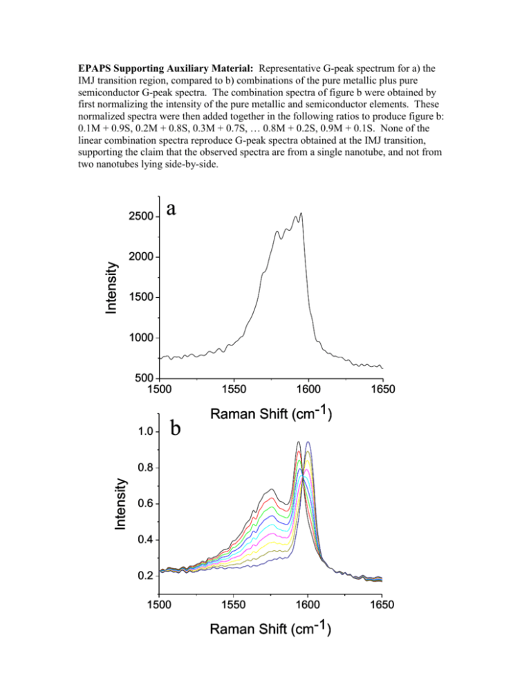
EPAPS Supporting Auxiliary Material: Representative G-peak spectrum for a) the IMJ transition region, compared to b) combinations of the pure metallic plus pure semiconductor G-peak spectra. The combination spectra of figure b were obtained by first normalizing the intensity of the pure metallic and semiconductor elements. These normalized spectra were then added together in the following ratios to produce figure b: 0.1M + 0.9S, 0.2M + 0.8S, 0.3M + 0.7S, … 0.8M + 0.2S, 0.9M + 0.1S. None of the linear combination spectra reproduce G-peak spectra obtained at the IMJ transition, supporting the claim that the observed spectra are from a single nanotube, and not from two nanotubes lying side-by-side. Intensity 2500 a 2000 1500 1000 500 1500 1.0 b 1550 1600 1650 Raman Shift (cm-1) Intensity 0.8 0.6 0.4 0.2 1500 1550 1600 Raman Shift (cm-1) 1650 A i i ii iii ii iii B C Tapping mode AFM images of nanotube IMJ transition region. A) 90 m segment (combined images of 3 X 30 m images) including highlighted M-S IMJ transition region. B) High resolution detail of IMJ transition region. C) Height profiles of transition region, showing the nanotube image is consistent with a single nanotube with unchanging diameter near 1.7 nm. Note the AFM image in Figure A is a small segment from a total length of 240 m that was probed by AFM on this nanotube. Only one nanotube is evident over the entire image. This is also consistent with AFM measurements of other long nanotubes present on our sample. All nanotubes greater than 100 ms in length exist as individual nanotubes and not as small bundles. Positioning overlap of the regions imaged in SEM, AFM, and Raman is made possible because the substrate has a number of large defects visible via SEM and also in white light images of the surface. Raman and AFM positioning can be correlated accurately to the position of these defect features. Additionally, the observed AFM and SEM features match exactly (compare figure 1 inset and above AFM image)—providing additional confidence that the targeted area has been imaged accurately. b Semicond. 12 a Position (m) 10 8 IMJ 6 4 2 0 144 145 146 147 148 RBM Frequency (cm-1) Metallic 100 120 140 Raman Shift 160 180 (cm-1) a) RBM frequency vs. position along the imaged nanotube for the data appearing in Figure 3a. Metallic to semiconducting character goes from high to low on the position axis. b) Plot of RBM spectra obtained from a second mapping scan of the IMJ region performed on a separate day. Within the +/- 1 cm-1 error in frequency for RBM peak position obtained from each individual spectrum (using a Lorentzian fitting routine to obtain peak position) no significant change in RBM frequency can be observed on moving from the metallic to semiconductor segment. Although the RBM weakens significantly (adding additional uncertainty to the semiconductor RBM frequency determination) on going to the semiconductor region of the nanotube, intensity does consistently appear for this mode for spectra taken on different days. 100 100 a b c 50 Intensity Intensity 0 Intensity 50 50 0 -50 -50 1300 1400 1500 1200 1300 -1 100 d 1500 1200 1300 -1 RamanShift (cm) 100 50 e 0 1400 1500 -1 RamanShift(cm) 100 f RamanShift (cm) 50 50 Intensity Intensity 1400 Intensity -50 1200 0 0 0 -50 -50 1200 1300 1400 1500 -50 1200 1300 1400 1500 1200 1300 1400 1500 Raman Shift (cm-1) Background subtracted D-peak region spectra from a,d) nanotube position corresponding to semiconductor region point “a” of Figure 2, b,e) position corresponding to the IMJ transition region point “d” of Figure 2, c,f) position corresponding to metallic region point “e” of Figure 2. The two sets of spectra were taken from different mapping scans on separate days. The weak peak at 1450 cm-1 is from the Si substrate. Its absence in Figure c and f is reproducible and is likely due to a minor defect occurring in the substrate at that point. The weak peak at 1308 cm-1 in Figure b appears to be spurious and cannot be identified as a D band with confidence.

