ch12
advertisement

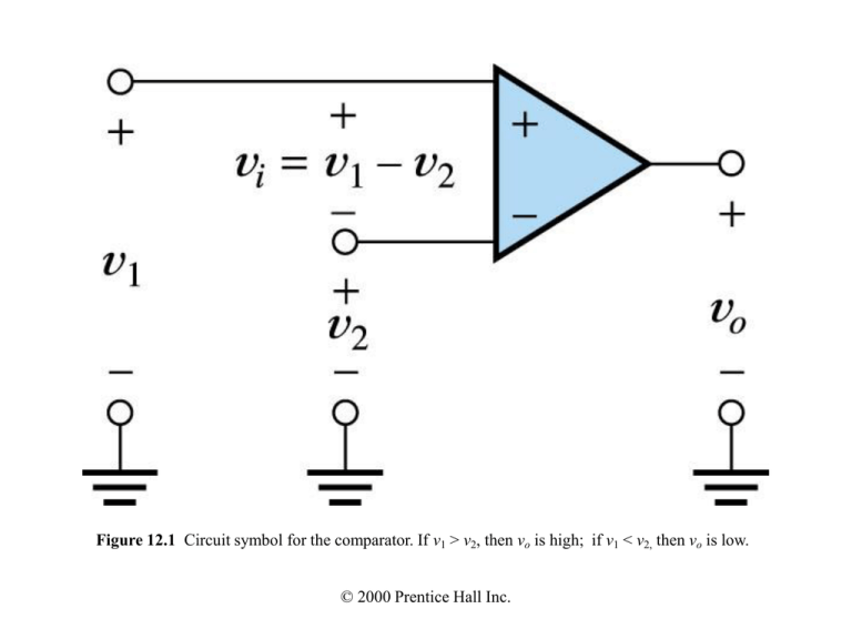
Figure 12.1 Circuit symbol for the comparator. If v1 > v2, then vo is high; if v1 < v2, then vo is low. © 2000 Prentice Hall Inc. Figure 12.2 Transfer characteristics of ideal comparators. © 2000 Prentice Hall Inc. Figure 12.3 Transfer characteristic of a real comparator. © 2000 Prentice Hall Inc. Figure 12.4 The LM111 has an open-collector output. © 2000 Prentice Hall Inc. Figure 12.5 The input voltage vin is compared to the reference voltage Vr. © 2000 Prentice Hall Inc. Figure 12.6 Noise added to the input signal can cause undesired transitions in the output signal. © 2000 Prentice Hall Inc. Figure 12.7 A Schmitt trigger is formed by using positive feedback with a comparator. © 2000 Prentice Hall Inc. Figure 12.8 Noninverting Schmitt trigger. © 2000 Prentice Hall Inc. Figure 12.9 Schmitt triggers that can be designed to have specified thresholds. © 2000 Prentice Hall Inc. Figure 12.10 Schmitt trigger designed in Example 12.1. © 2000 Prentice Hall Inc. Figure 12.11 Input voltage and output voltage versus time for the circuit of Figure 12.10. © 2000 Prentice Hall Inc. Figure 12.12 Transfer characteristic for the Schmitt trigger of Example12.1. © 2000 Prentice Hall Inc. Figure 12.13 Answer for Exercise12.1. © 2000 Prentice Hall Inc. Figure 12.14 Answer for Exercise 12.2. © 2000 Prentice Hall Inc. Figure 12.15 Answer for Exercise 12.3. © 2000 Prentice Hall Inc. Figure 12.16a Astable multivibrator. © 2000 Prentice Hall Inc. Figure 12.16b Astable multivibrator. © 2000 Prentice Hall Inc. Figure 12.17 Waveforms of Figure 12.16b with t = 0 at the start of a positive half-cycle of vo(t). © 2000 Prentice Hall Inc. Figure 12.18 Astable multivibrator designed in Example 12.3. © 2000 Prentice Hall Inc. Figure 12.19 Simulated voltages for the circuit of Figure 12.18. © 2000 Prentice Hall Inc. Figure 12.20 Circuit for Exercise 12.5. © 2000 Prentice Hall Inc. Figure 12.21 Answer for Exercise 12.5b. © 2000 Prentice Hall Inc. Figure 12.22 Circuit for Exercise 12.6. © 2000 Prentice Hall Inc. Figure 12.23 Answer for Exercise 12.6b. © 2000 Prentice Hall Inc. Figure 12.24 Simplified functional block diagram of 555 timer IC. © 2000 Prentice Hall Inc. Figure 12.25 Monostable multivibrator. © 2000 Prentice Hall Inc. Figure 12.26 Astable oscillator. © 2000 Prentice Hall Inc. Figure 12.27 Circuit for Exercises 12.7 and 12.8. © 2000 Prentice Hall Inc. Figure 12.28 Simple rectifier circuits such as this are not suitable for precision rectification of small-amplitude ac signals. © 2000 Prentice Hall Inc. Figure 12.29a Precision half-wave rectifier. © 2000 Prentice Hall Inc. Figure 12.29b Precision half-wave rectifier. © 2000 Prentice Hall Inc. Figure 12.30 Improved half-wave rectifier. © 2000 Prentice Hall Inc. Figure 12.31 Precision full-wave rectifier. © 2000 Prentice Hall Inc. Figure 12.32 See Exercise 12.10. © 2000 Prentice Hall Inc. Figure 12.33 Simple peak detector. © 2000 Prentice Hall Inc. Figure 12.34 Precision peak detector. © 2000 Prentice Hall Inc. Figure 12.35 Answers for Exercise 12.13. © 2000 Prentice Hall Inc. Figure 12.36a Sample-and-hold circuit. © 2000 Prentice Hall Inc. Figure 12.36b Sample-and-hold circuit. © 2000 Prentice Hall Inc. Figure 12.37a Precision clamp circuit. © 2000 Prentice Hall Inc. Figure 12.37b Precision clamp circuit. © 2000 Prentice Hall Inc. Figure 12.38a Answers for Exercise 12.14. © 2000 Prentice Hall Inc. Figure 12.38b Answers for Exercise 12.14. © 2000 Prentice Hall Inc. Figure 12.39 Analog-to-digital conversion. © 2000 Prentice Hall Inc. Figure 12.40 The DAC output is a staircase approximation to the original signal. Filtering removes the sharp corners. (Note: In addition to smoothing, the filter delays the signal. The delay is not shown.) © 2000 Prentice Hall Inc. Figure 12.41 Circuit symbol for a digital-to-analog converter. © 2000 Prentice Hall Inc. Figure 12.42 DACs can be implemented using a weighted-resistance network. (Note: If di = 1, the corresponding switch is to the right-hand side. For di = 0, the i th switch is to the left-hand side.) © 2000 Prentice Hall Inc. Figure 12.43 An R -- 2R ladder network. The resistance seen looking into each section is 2R. Thus, the reference current splits in half at each node. © 2000 Prentice Hall Inc. Figure 12.44 An n-bit DAC based on the R–2R ladder network. © 2000 Prentice Hall Inc. Figure 12.45 A practical n-bit DAC based on BJT technology that uses emitter-coupled pairs as current switches. © 2000 Prentice Hall Inc. Figure 12.46a Switched-capacitance DACs. © 2000 Prentice Hall Inc. Figure 12.46b Switched-capacitance DACs. © 2000 Prentice Hall Inc. Figure 12.47 Conceptual block diagram of an analog-to-digital converter. © 2000 Prentice Hall Inc. Figure 12.48 A flash converter. © 2000 Prentice Hall Inc. Figure 12.49 Output versus input for a 3-bit ADC. © 2000 Prentice Hall Inc. Figure 12.50a Dual-slope ADC. © 2000 Prentice Hall Inc. Figure 12.50b Dual-slope ADC. © 2000 Prentice Hall Inc. Figure 12.51a Successive approximation ADC. © 2000 Prentice Hall Inc. Figure 12.51b Successive approximation ADC. © 2000 Prentice Hall Inc.


