W12_Slides
advertisement
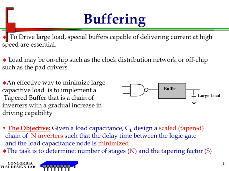
Buffering To Drive large load, special buffers capable of delivering current at high speed are essential. Load may be on-chip such as the clock distribution network or off-chip such as the pad drivers. An effective way to minimize large capacitive load is to implement a Tapered Buffer that is a chain of inverters with a gradual increase in driving capability Buffer Large Load • The Objective: Given a load capacitance, CL design a scaled (tapered) chain of N inverters such that the delay time between the logic gate and the load capacitance node is minimized The task is to determine: number of stages (N) and the tapering factor (S) CONCORDIA VLSI DESIGN LAB 1 OUTPUT Pad and Driver CONCORDIA VLSI DESIGN LAB 2 CLOCK DRIVER CONCORDIA VLSI DESIGN LAB 3 Buffering S = scaling or tapering factor CL = SN+1 Cg ……………… CONCORDIA VLSI DESIGN LAB All inverters have identical delay of to = delay of the first stage (load =Cd+Cg) 4 Buffering If the diffusion capacitance Cd is neglected, then S = e = 2.7 5 S 4 3 0 CONCORDIA VLSI DESIGN LAB 1 2 3 Cd/Cg 5 Layout of a standard inverter Diffusion Polysilicon Metal Wp Vin PMOS Vo Wn L NMOS VSS CONCORDIA VLSI DESIGN LAB 6 Layout of Large Device •Drain-Source Area •Delay of Gate CONCORDIA VLSI DESIGN LAB 7 Layout of a Buffer D(rain) S Multiple Contacts D G S(ource) S G(ate) (a) small transistors in parallel CONCORDIA VLSI DESIGN LAB (b) circular transistors 8 Prentice Hall/Rabaey Large Transistor Layout Increase # of Contacts CONCORDIA VLSI DESIGN LAB 9 Output Drivers Standard CMOS Driver Open Drain/Source Driver: Single Transistors Tri-state Driver Bi-directional Circuit CONCORDIA VLSI DESIGN LAB 10 Output Drivers Bonding Pad GND 100 mm Out Out VDD CONCORDIA VLSI DESIGN LAB In GND 11 Prentice Hall/Rabaey Tri-state Driver Tri-state or High impedance Used to drive internal or external busses Two inputs: Data In and Enable Various signal assertions En Two types: In C2MOS En CMOS with Control Logic VDD Out C2MOS CONCORDIA VLSI DESIGN LAB 12 Tri-state Driver VDD Control logic could be modified to obtain En Inversion/non-inversion Active low/high Enable Out For large load, pre-drivers are required PAD En In CONCORDIA VLSI DESIGN LAB 13 Latch-up on CMOS Inherent in bulk CMOS processes are parasitic bipolar transistors forming p+/n /p /n+ path between VDD and VSS The four layer path is equivalent to SCR which when triggered can cause self sustaining latch-up between power supplies resulting in total or local destruction. VDD VSS n+ p+ p+ n+ T1 Rw n+ VDD p+ Rs T2 T2 P-well Rs Drain of PMOS Drain of NMOS T1 Rw n-substrate Vss CONCORDIA VLSI DESIGN LAB 14 Latch-up: Analysis If VA>VDD+0.6, T1 will be turned ON Ic1 causes a voltage drop across Rw If V(Rw) > 0.6V V, T2 will be turned ON, this forces Ic2 to be supplied by VDD through n+ substrate contact, then the bulk to p-well. Increase in voltage across Rs causes and in increase in Ic1, hence sustaining SCR action. The same action will take place when: VB< -0.6V Hence to prevent latch-up, limit the output voltage -0.6< Vout < VDD+0.6V VDD IE1 Rs IB1 IC1 VA T1 IC1 T2 IB2 VB Rw IE1 VSS CONCORDIA VLSI DESIGN LAB 15 Latch-up: Trigger Factors which trigger latch-up transmission line reflections or ringing voltage drop on the VDD bus “hot plug in” of unpowered circuit board electrostatic discharge sudden transient on power and ground busses leakage current across the junction radiation: x-ray, cosmic CONCORDIA VLSI DESIGN LAB 16 Latch-up: Prevention 1. Layout techniques: Incorporate collectors for latch-up current: Create diffused n and p guard rings that surround active devices These collectors can sink the current but are incapable of sustaining the latch-up mechanism once the cause is removed guard ring n+ p+ CONCORDIA VLSI DESIGN LAB n+ n+ p+ p+ n+ p+ GND 17 Input protection Electrostatic discharge can take place through transfer of charges from the human body to the device. Human body can carry up to 8000V. Discharge can happen within hundreds of nanoseconds. Critical field for SiO2 is about 7X10⁶ V/cm. For 0.5u CMOS process the gate oxide can withstand around 8V Some protection technique is required with minimum impact on performance 1.5K 1M Vesd DUT 100pF Human Body model CONCORDIA VLSI DESIGN LAB 18 Input PAD CONCORDIA VLSI DESIGN LAB 19 Protection Circuitry Principles Punch Through CONCORDIA VLSI DESIGN LAB Avalanche 20 Vd d Input Pad Circu it Vs s CONCORDIA VLSI DESIGN LAB 21 ESD Structures Basic technique is to include series resistance and two clamping diodes. The resistance R is to limit the current and to slow down the high voltage transitions. R could be polysilicon or diffusion resistance Diffusion resistance could be part of the diode structure Typical values of R: 500 to 1k VDD R PAD CONCORDIA VLSI DESIGN LAB 22 Protection Circuitry Based on gate modulated junction breakdown CONCORDIA VLSI DESIGN LAB 23 Protection Circuitry CONCORDIA VLSI DESIGN LAB 24 Layout of ESD Structure This structure uses transistors as clamping diodes PAD n+ p+ Guard Ring Guard Ring p+ p+ CONCORDIA VLSI DESIGN LAB n+ n+ 25 Layout of ESD Structure VDD PAD n+ p+ Guard Ring Guard Ring p+ p+ n+ n+ GND CONCORDIA VLSI DESIGN LAB 26 Guard Rings for critical Transistors VDD Vin Diffusion n+ N Contact Vss Polysilico Diffusion P+ n CONCORDIA VLSI DESIGN LAB Metal 27 VDD CONCORDIA VLSI DESIGN LAB 28 Structure of a P+ Diode VDD N+ Guard N Sub M1 P+ Input CONCORDIA VLSI DESIGN LAB OUTPUT 29 Another ESD Structure VDD PAD R1 R2 Thick FOX MOS Transistor CONCORDIA VLSI DESIGN LAB 30 Bi-direct PAD VDD Pre-drivers IN EN ESD Protection Input Buffer Control Logic CONCORDIA VLSI DESIGN LAB PAD 31 D2 D3 R PAD D1 D2 D3 D1 D4 R N+ P substrate CONCORDIA VLSI DESIGN LAB P+ N-Well SiO2 N+ @ VDD connected to Gnd 1X D4 Metal– to CCT 4X 2D vs. 2.5D vs. 3D ICs 101 By: Clive Maxfield 4/8/2012 12:08 PM EDT Birds-eye view of circuit board with individually packaged chips Birds-eye view of circuit board with a System-in-Package (SiP) device CONCORDIA VLSI DESIGN LAB Birds-eye view of circuit board with a System-on-Chip (SoC) device Birds-eye view of circuit board with a System-in-Package (SiP) device 33 3D Structures 2D vs. 2.5D vs. 3D ICs 101 By: Clive Maxfield 4/8/2012 12:08 PM EDT A simple form of 3D IC/SiP Connecting dice using wires running down the sides 3D stack A more complex “True 3D IC/SiP A simple “True 3D IC/SiP” CONCORDIA VLSI DESIGN LAB 34 Thank you ! CONCORDIA VLSI DESIGN LAB 35
