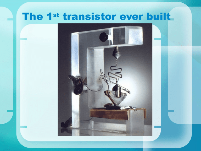
The 1st transistor ever built Transistor operation DC DC biasingbiasingBJTs BJTs S.R.R.Govt.Arts & Science College, KNR Topics objectives • You’ll learn • Q-point of a transistor operation • About DC analysis of a transistor circuit • About Transistor biasing configuration • Other available transistor biasing circuits • Stability factor for transistor • Transistor switching INTRODUCTION • BJTs amplifier requires a knowledge of both the DC analysis (LARGE-signal) and AC analysis (small signal). • For a DC analysis a transistor is controlled by a number of factors including the range of possible operating points. • Once the desired DC current and voltage levels have been defined, a network must be constructed that will establish the desired operating point. • BJT need to be operate in active region used as amplifier. • The cutoff and saturation region used as a switches. • For the BJTs to be biased in its linear or active operating region the following must be true: a) BE junction forward biased, 0.6 or 0.7V b) BC junction reverse biased INTRODUCTION(CONTINUED) • DC bias analysis assume all capacitors are open cct. • AC bias analysis : 1) Neglecting all of DC sources 2) Assume coupling capacitors are short cct. The effect of these capacitors is to set a lower cut-off frequency for the cct. 3) Inspect the cct (replace BJTs with its small signal model). 4) Solve for voltage and current transfer function and i/o and o/p impedances. • For transistor amplifiers the resulting DC current and voltage establish an operating point that define the region that can be employed for amplification process. Various operating points within the limits of operation of a transistor Q-point C: • Concern on nonlinearities due to I B curves is rapidly changes in this region. I Cmax IC(mA) B: PCmaxQ-point IB=60 bestuAoperating point • The 18 for linear gain and largest and current possible IB=50 voltage uA • It is a desired condition for IB=40signal uA analysis a small 15 Saturation 12 B 9 Q-point A: • I=0A, V=0V • Not suitable for transistor to operate IB=30 uA IB=20 uA 6 IB=10 uA C 3 IB=0 uA A VCEsat VCE(V) 10 20 Cutoff 30 40 VCEmax FIXED-BIAS CCT VCC VCC IC RC RB AC input signal IB C1 C B + VBE E - VCC IC C2 + VCE - AC output signal RB IB C B + VBE E - C1,C2 = coupling capacitors AC ANALYSIS DC ANALYSIS RC + VCE - EMITTER-STABILIZED BIAS CCT VCC IC RC RB Vo IB Vi C2 C1 IE Fig. 5.11 RE Voltage divider bias VCC RC R1 Vo C2 Vi C1 R2 RE Fig. 5.18: Voltage-divider bias configuration Forward Bias of Base-Emitter • Refer to fig. 5.1. This cct also known as input loop. + VCC - RB IB C B + VBE E - + VCE - Use KVL : VCC - IBRB - VBE 0 rearrange the eq above we get, VCC - VBE IB RB known that IC IB thus equ. above can rearrange as follows : VCC - VBE I C Fig. 5.1 : Base-emitter loop RB Collector-Emitter Loop • Refer to fig. 5.2. Also known as output loop. Use KVL : VCC - ICRc - VcE 0 VcE VCC - ICRc known that VcE VC - VE, since VE 0 V IC + RC C + VCE - VCC Fig. 5.2 : Collector-emitter loop thus we get, VCE VC. Also known that VBE VB - VE, since VE 0V, thus we get, VBE VB The value of IC, IB and VCE shows the position of Q-point at o/p graph. The notation of this value changes to ICQ, IBQ and VCEQ. Example 1: Determine the following for the fixed bias configuration of Fig 5.3. a) IBQ and ICQ b) VCEQ c) VB and VC d) VBC VCC=+12V IC RB=240kohm AC input signal C1 IB 10uF RC=2.2kohm C2 C B + VBE E - Fig. 5.3 AC output signal + 10uF VCE 50 Solution VCC VBE RB 12 0.7 47.08uA 240k a ) IBQ ICQ IBQ 50 47.08u 2.34 mA b) VCEQ VCC - ICRC 12 - 2.35m 2.2k 6.83V c) VBE VB 0.7 V VCE VCEQ VC 6.83 V d )VBC VB VC 0.7 6.83 6.13V - ve sign indicates that BC - junction is reverse biased. Example 2: Determine the following for the fixed bias configuration of Fig 5.4. a) IBQ and ICQ b) VCEQ c) VB d)VC e) VE VCC=+16V IC RB=470kohm IB C B + VBE 90 E - Fig. 5.4 RC=2.7kohm + VCE - Solution VCC VBE RB 16 0.7 32.55uA 470k a ) IBQ ICQ IBQ 90 32.55u 2.93 mA b) VCEQ VCC - ICRC 16 - 2.93m 2.7 k 8.17V c) VBE VB 0.7 V d)VCE VCEQ VC 8.17 V e)VE 0V Transistor Saturation • Saturation means the level of systems have reached their maximum values. • For a transistor operating in the saturation region, the current is maximum value for a particular design. • Saturation region are normally avoided because the B-C junction is no longer reverse-biased and the o/p amplified signal will be distorted. • Fig 5.5 shows the schematic diagram to determine ICsat for the fixed-bias configuration. The saturation current for the fixed bias configuration is: VCC RB + RC V =V - RC CC ICsat VCC + VCE=0V - Fig. 5.5 ICsat RC Example 3: By refering to example 1 and Fig. 5.3 determine the saturation level. Solution: ICsat VCC 12 5.45mA RC 2 .2 k The design of example 1 in ICQ 2.34mA. It can be concluded that the ICQ is operates within the limit. Example 4: Find the saturation current for the fixed-bias configuration of Fig. 5.4. Solution: ICsat VCC 16 5.92mA RC 2.7 k The design of example 2 in ICQ 2.93mA. It can be concluded that the ICQ is operates within the limit. Load line analysis • By refering to Fig. 5.2 (output loop) one straight line can be draw at output characteristics. This line is called load line. • This line connecting each separate of Q-point. • At any point along the load line, values of IB, IC and VCE can be picked off the graph. • The process to plot the load line as follows: Step 1: Refer to fig. 5.2, VCE=VCC – ICRC (1) Choose IC=0 mA. Subtitute into (1), we get VCE=VCC (2) located at X axis Step 2: Choose VCE=0V and subtitute into (1), we get IC=VCC/RC (3) located at Y-axis Step 3: Joining two points defined by (2) + (3), we get straight line that can be drawn as Fig. 5.6. IC(mA) VCC/RC VCE=0 V Fig. 5.6 Load line Q-point IBQ VCE(V) VCC IC=0 mA Case 1: IC(mA) VCC/RC • Level IB changed by varying the value of RB. • Q-point moves up and down IBQ3 Q-point Q-point IBQ2 Q-point IBQ1 VCE(V) VCC Fig. 5.7:Movement of Q-point with increasing levels of IB IC(mA) Case 2: VCC/RC1 VCC/RC2 RC3 > RC2 > RC1 VCC/RC3 Q-point Q-point IBQ Q-point VCE(V) VCC Fig. 5.8 : Effect of increasing levels of RC on the load line and Q-point • VCC fixed and RC change the load line will shift as shown in Fig 5.8 • IB fixed, the Q-point will move as shown in the same figure. IC(mA) Case 3: VCC1/RC VCC1 > VCC2 > VCC3 VCC2/RC VCC3/RC Q-point Q-point IBQ Q-point VCE(V) VCC3 VCC2 VCC1 Fig. 5.9: Effect of lower values of VCC on the load line and Q-point • RC fixed and VCC varied, the load line shifts as shown in Fig. 5.9 Example 5: Given the load line of Fig. 5.10 and defined Q-point, determine the required values of VCE, RC and RB for a fixed bias configuration. IC(mA) IB=60 uA ICmax 18 IB=50 uA 15 IB=40 uA 12 9 IB=30 uA 6 IB=20 uA Q-point IB=10 uA 3 IB=0 uA VCE(V) 10 20 30 Fig. 5.10 40 Solution: Step 1 : VCE VCC 40 V at IC 0 mA VCC at VCE 0V. RC VCC 40 RC 2.67 kohm IC 15m IC Step 2 : VCC - VBE IB RB VCC VBE RB IB 40 0.7 17 2311 kohm Example 6: Determine the value of Q-point for Fig. 5.11. Also find the new value of Q-point if change to 150. VCC=+12V IC RB=100kohm IB C B + VBE 100 E - Fig. 5.11 RC=560ohm + VCE - Solution: Step 1 : 100, 12 - 0.7 113 A 100k IC IB 100 113 11.3 mA IB Step 2 : VCE VCC - ICRC 12 - 11.3m 560 5.67 V Q po int 5.67 V,11.3mA Step 3 : new 150, 12 - 0.7 IB 113 A the value is same, 100k IC IB 150 113 16.95 mA Step 4 : VCE VCC - ICRC 12 - 16.95m 560 2.51V New Q - point (2.51 V, 16.95mA) Thechange changeof of The causethe the cause bigchange changeof of big Q-pointvalue. value. Q-point Thisshows shows This thatfixed fixed that biased biased configuration configuration NOTstable stable isisNOT • • a) b) EMITTER-STABILIZED BIAS CCT The DC bias network of Fig 5.12 contains an emitter resistor to improve the stability level of fixed-bias configuration. The analysis consists of two scope: Examining the base-emitter loop (i/p loop) Use the result to investigate the collector-emitter loop (o/p loop) VCC IC RC RB Vo IB Vi C2 C1 IE Fig. 5.11 RE Base-Emitter Loop (i/p loop) • Refer to fig. 5.12. KVL : VCC - IBRB - VBE - IERE 0 (1) known that IE 1 IB, subtitute into (1) we get, + VCC - RB IB VCC - IBRB - VBE - 1 IBRE 0 B + VBE Rearrange the equ, finally we get, E IE RE Fig. 5.12 : Base-emitter loop VCC - VBE IB RB 1 RE Collector-Emitter Loop (o/p loop) • Refer to fig. 5.13. KVL : VCC - ICRC - VCE - IERE 0 IC + RC Assuming IE IC rearrange equ (1) we get, C IE + VCE - (1) VCC VCE VCC - IC(RC RE) From the Fig.5.13 we also can know VE IERE RE VCE VC - VE Fig. 5.13 : Collector-emitter loop VC VCE VE OR VB VCC - IBRB OR VC VCC - ICRC VB VBE VE Example 7: For the emitter-bias network fo Fig.5.14 determine: a)IB b)IC c)VCE d)VC e)VE f)VB g)VBC VCC=+20V IC RC=2 kohm RB=430kohm IB 50 IE Fig. 5.14 RE=1 kohm Solution: a) IB VCC - VBE 20 0.7 40.1A RB 1 RE 430k 50 11k b) IC IB 50 40.1 2.01mA c) VCE VCC - IC RC RE 20 2.01m 2k 1k 20 6.03 13.97 V d ) VC VCC ICRC 20 2.01m 2k 20 4.02 15.98V e) VE VE VCE 15.98 13.97 2.01V OR VE IERE ICRE 2.01m 1k 2.01V f ) VB VBE VE 0.7 2.01 2.71V g ) VBC VB VC 2.71 15.98 13.27 V (reverse biased as required) Improved Bias Stability Issues: Comparison analysis for example 1 and example 7. Data from example 1 (fixed-bias configuration) IB(A) IC(mA) VCE(V) 50 100 47.08 47.08 2.35 4.71 6.83 1.64 Data from example 7 (emitter-bias configuration) IB(A) IC(mA) VCE(V) 50 100 40.1 36.3 2.01 3.63 13.97 9.11 Takehome exercise: For the emitter-stabilized biase cct of Fig. 5.15, determine IBQ, ICQ, VCEQ, VC, VB, VE. VCC=+20V IC RC=2.4 kohm RB=510kohm IB 100 Fig. 5.15 IE RE=1.5 kohm Saturation The saturation current for an emitter-bias configuration is: VCC + RC Fig. 5.16 - ICsat + VCE=0V - RE VCC ICsatRC ICsatRE 0 VCC ICsat RC RE 0 VCC ICsat RC RE Example 8: Determine the saturation current for the network of example 7. Solution: ICsat VCC RC R E 20 20 6.67mA 2k 1k 3k This value is about three times the level of ICQ (2.01mA =50) for the example 7. Its indicate the parameter that been used in example 7 can be use in analysis of emitter bias network. Load line analysis • The process to plot the load line as follows: Step 1: Refer to fig. 5.13, VCE=VCC – IC(RC+RE) (1) Choose IC=0 mA. Subtitute into (1), we get VCE=VCC (2) located at X axis Step 2: Choose VCE=0V, subtitute into (1) gives VCC IC RC RE VCE 0V (3) located at Y axis Step 3: Joining two points defined by (2) + (3), we get straight line that can be drawn as Fig. 5.17: IC VCC/(RC+RE) Q-point ICQ IBQ VCE(V) VCEQ VCC Fig. 5.17: Load line for the emitter-bias configuration VOLTAGE-DIVIDER BIAS Data from example 7 IB(A) IC(mA) VCE(V) 50 100 40.1 36.3 2.01 3.63 13.97 9.11 • ICQ and VCEQ from the table of example 7 is changing dependently the changing of . • The voltage-divider bias configuration such as in Fig. 5.18 is designed to have a less dependent or independent of the . • If the cct parameter are properly choosen, the resulting levels of ICQ and VCEQ can be almost totally independent of . VCC • Two method for analyzed the voltage-divider bias configuration: a) Exact method b) Approximate method RC R1 Vo C2 Vi C1 R2 RE Fig. 5.18: Voltage-divider bias configuration Exact Analysis Step 1: • The i/p side of the network of Fig. 5.18 can be redrawn as shown in Fig. 5.19 for DC analysis. Step 2: • Analysis of Thevenin equivalent network to the left of base terminal R 1 VCC R2 RE Thevenin Fig. 5.19: Redrawn the i/p side of the network of Fig 5.18 Exact Analysis Step 2(a): Replaced the voltage sources with short-cct equivalent as shown in Fig 5.20 and gives us the value of RTH R1 RTH R 1 R 2 R2 RTH Fig. 5.20: Determining RTH Exact Analysis Step 2(b): Determining the ETH by replaced back the voltage sources and open cct Thevenin voltage as shown in Fig. 5.21. Then apply the voltage-divider rule. R1 VCC R2 + + VR2 ETH - - Fig. 5.21: Determining ETH ETH VR 2 R 2 VCC R1 R 2 Exact Analysis Step 3: The Thevenin network is then redrawn as shown in Fig. 5.22 and IBQ can be determined by KVL RTH IB ETH + VBE ETH IBRTH VBE IERE 0 - IE Fig. 5.22: Inserting the Thevenin equivalent cct. RE Subtitute IE β 1 IB gives ETH VBE IB RTH 1 RE Example 9:Determine the DC bias voltage VCE and current IC for the voltage-divider configuration of network below: VCC=22V R1=39kohm RC=10kohm 140 R2=3.9kohm RE=1.5kohm Solution: RTH R 1 R 2 39k 3.9k 3.55 kohm 39k 3.9k ETH R 2 VCC 3.9k 22 2V R1 R 2 39k 3.9k ETH VBE IB RTH 1 RE 2 0 .7 6.05A 3.55k 140 11.5k IC IB 140 6.05 0.85mA VCE VCC IC RC RE 22 0.85m10k 1.5k 12.22V Example 10: For the voltage-divider bias configuration of Fig. 5.23, determine: IBQ, ICQ, VCEQ, VC, VE and VB. VCC=16V ICQ R1=62kohm RC=3.9kohm IBQ 80 RE=0.68kohm R2=9.1kohm Fig. 5.23 Solution: RTH R 1 R 2 62k 9.1k 7.93 kohm 62k 9.1k VCEQ VCC IC RC RE 16 1.712m 3.9k 0.68k 8.16V R 2 VCC 9.1k 16 ETH 2.05V R 1 R 2 62k 9.1k VC VCC ICRC 16 1.712m 3.9k 9.32V ETH VBE IBQ RTH 1 RE 2.05 0.7 21.4A 7.93k 80 1 0.68k VE IERE IB IC 0.68k 21.4 1.712m 0.68k ICQ IB 80 21.4 1.712mA VB VE VBE 1.18 0.7 1.88V 1.18V Approximate Analysis Step 1: RE 10R2 Step 2: The i/p section can be represented by the network of Fig. 5.24. R1 and R2 can be considered in series by assuming I1I2 and IB= 0A . I1 R1 IB VCC + I2 VB R2 - Ri Ri R 2 I1 I 2 Ri 1 RE Fig. 5.24: Partial-bias cct for calculating the approximate base voltage, VB Approximate Analysis Step 3: The base voltage can be determined : I1 R2VCC VB VR2 R 1 R2 R1 IB VCC + I2 VB R2 Ri - and level VE can be calculated as well : VBE VB - VE VE VB - VBE Fig. 5.24: Partial-bias cct for calculating the approximate base voltage, VB and the emitter current can be determined : IE VE and ICQ IE RE Condition that will define approximate approach : βR E 10R 2 where R i ( 1)R E R E NPN Transistor simulation Example 11:Repeat the analysis of example 9 using the approximate technique and compare solution for ICQ and VCEQ. Solution: Step1 : RE 10R 2 1401.5k 10 3.9k 210kohm 39kohm satisfied! Step 2 : the partial bias cct can be drawn Step 3 : R 2 VCC 3.9k 22 VB 2V R 1 R 2 39k 3.9k VE VB VBE 2 0.7 1.3V VE 1.3 ICQ IE 0.867 mA RE 1.5k VCEQ VCC IC RC RE 22 0.867 m10k 1.5k 12.03V ICQ(mA) VCEQ(V) Exact Analysis 0.85 12.22 Approxima te Analysis 0.867 12.03 ICQ and VCEQ are certainly close. Example 12:Repeat the exact analysis of example 9 if is reduced to 70. Compare the solution for ICQ and VCEQ. Solution: RTH 3.55 kohm ETH 2V ETH VBE RTH 1 RE 2 0.7 11.81A 3.55k 70 11.5k IB IC IB 7011.81 0.83mA Solution (continued): VCE VCC IC RC RE 22 0.83m10k 1.5k 12.46V ICQ(mA) VCEQ(V) 140 0.85 12.22 70 0.83 12.46 Conclusion: Even though is drastically half, the level ICQ and VCEQ are essentially same. Example 13:Determine the levels of ICQ and VCEQ for the voltage-divider configuration fo Fig. 5.25 using the exact and approximate analysis. Compare the solution. VCC=18V ICQ R1=82kohm RC=5.6kohm IBQ R2=22kohm 50 Fig. 5.25 RE=1.2kohm Solution: Exact Analysis : RTH R 1 R 2 82k 22k 17.35 kohm 82k 22k ETH R 2 VCC 22k 18 3.81V R 1 R 2 82k 22k ETH VBE IBQ RTH 1 RE 3.81 0.7 39.6A 17.35k 50 11.2k ICQ IB 50 39.6 1.98mA VCEQ VCC IC RC RE 18 1.98m 5.6k 1.2k 4.54V Solution (continued): Approximate Analysis : RE 10R 2 501.2k 10 22k 60kohm 220kohm (not satisfied) R 2 VCC 22k 18 3.81V R 1 R 2 82k 22k VE VB VBE 3.81 0.7 3.11V VB ETH VE 3.11 ICQ IE 2.59mA RE 1.2k VCEQ VCC IC RC RE 18 2.59m 5.6k 1.2k 3.88V Solution (continued): Exact Analysis ICQ(mA ) %differen VCEQ(V) %differen ce ce 1.98 4.54 Approximat 2.59 e Analysis 23.5% 17% 3.88 The saturation collector-emitter cct for the voltage-divider configuration has the same appearance as the emitterbiased configuration as shown in Fig. 5.27 VCC VCC ICsat RC RE + RC Fig. 5.27 - ICsat + VCE=0V - RE Load line analysis • The similarities with the o/p cct of the emitter-biased configuration result in the same intersections for the load line of the voltage-divider configuration. • The load line therefore have the same appearance with: VCC IC RC R E VCE 0V located at Y axis VCE VCC IC0mA located at X axis DC Bias with Voltage Biasing Another way to improve the stability of a bias circuit is to add a feedback path from collector to base. In this bias circuit the Q­point is only slightly dependent on the transistor Beta . Base-Emitter Loop Applying Kirchoff’s voltage law: VCC – ICRC – IBRB – VBE –IERE = 0 Note: IC = IC + IB ­­ but usually IB << IC ­­ so IC IC Knowing IC = IB and IE IC then: VCC – IB RC – IBRB – VBE –IBRE = 0 VCC VBE I B Simplifying and solving for IB: RB (RC RE) Collector-Emitter Loop Applying Kirchoff’s voltage law: IE + VCE + ICRC – VCC = 0 Since IC IC and IC = IB: IC(RC + RE) + VCE – VCC =0 Solving for VCE: VCE VCC I C ( RC RE ) Transistor Saturation Level VCC ICsat ICmax RC RE Load Line Analysis It is the same analysis as for the voltage divider bias and the emitter­biased circuits. Simulation of a NPN type common-emitter transistor Design Operation • We are able to design the transistor circuit using the ideas that we have learnt before during analyzing dc biasing circuit. • How? – Understand the Kirchof’s Law and other electric circuit law such as Ohms Law, Thevenin Laws etc – Identify the parameters given – Analyze into the input/output for the system and build a loop using electric circuit’s law. Miscellaneous configuration Examples Examples Examples of design • Design of a bias circuit with an emitter feedback resistor • Design of a current-gainstabilized circuit (beta independent) Design of a bias circuit with an emitter feedback resistor The emitter resistor is ¼ to 1/10 of the supply voltage Design of a current-gain-stabilized circuit (beta independent) The emitter resistor is ¼ to 1/10 of the supply voltage To determine R1 and R2 use 10R2≤βRE Transistor as switching networks • Transistor works as an inverter in computer circuits. • Operating point switch from cut-off to saturation along the load line for proper inversion. • In order to understand, we assume that; • IC=ICEO=0mA • VCE=Vsat=0V • One must understand the transistor graph output and load-line analysis to describe and discuss about the transistor switching networks. Transistor as a switch We mustensurethat IB ICsat compare withthe figure, we'll see that, V 0.7 IB I 63uA 68k V ICsat cc 6.1mA RC Therefore,IB ICsat 6.1mA 48.8uA 125 Time interval Time interval continued Troubleshooting? • How to define and encounter transistor circuit problem? PNP configuration Bias stabilization • Stability of a system is a measure of the sensitivity of a network to variation in its parameter. – β increases with increase in temperature – VBE decreases 7.5mV every degree celcius – ICO doubles every 10 oC increase in temperature Effect of non-stability circuit/system Room temperature 100oC temperature We’ll find that β increase after 100OC, base current is same but not suitable to use due it is very near to the saturation region. Stability factors IC S(ICO ) ICO IC S(VBE) VBE IC S( ) S(ICO) • Emitter bias configuration RB ) RE S(ICO ) ( 1) R ( 1) ( B ) RE 1 ( If RB RE ( 1), it willreduce to S(ICO ) ( 1) If RB RE ( 1), it willreduce to S(ICO ) 1 For ranges of RB RE from1to 1, stability factor willbe , S(ICO ) RB RE • Fixed bias configuration S(ICO) RB 1 ( ) RE S(ICO ) ( 1) R ( 1) ( B ) RE If multiplying above equation withREfor the numerator and denumerator,and assumeRE 0 we'll obtain, S(ICO ) ( 1)....so it'snot stable and reach the maximumvalue • Voltage divider bias configuration RTh ) RE S(ICO ) ( 1) R ( 1) ( Th) RE 1 ( Thisissame to the emitter- bias configuration characteristic,but differsonly because analyze usingTheveninrule. • Feedback bias configuration S(ICO) RB ) RC S(ICO ) ( 1) R ( 1) ( B ) RC 1 ( Where RE 0 • Physical impact Fixed bias configuration ; IC=βIB+(β+1)ICO...IC increase but IB maintain, so it’s not stable Emitter bias configuration ; Increase IC will increase ICO. It affect VE since VE=IERE=ICRE. In turn, the output loop will inform that IB will decrease if VE is increase, thus affect to reduce the collector current. Feedback bias configuration ; same as result of emitter bias configuration where IB will decrease if IC increase. (IC proportional to VRC) Voltage divider bias configuration ; Most stable where as long as 10R2>> βRE, VB remain constant for any changing in IC. S(VBE) IC S(VBE) VBE RB ( 1)RE ......(if RE 0) RB or RE RB ( 1) RE 1 ......(if 1 RB ) RE RE S(β) IC S( ) RB ) RE IC R 1(1 2 B ) RE IC (1 References: 1. 2. 3. 4. Thomas L. Floyd, “ Electronic Devices, Sixth edition”, Prentice Hall, 2002. Robert Boylestad, “Electronic Devices and Circuit Theory”, Eighth edition, Prentice Hall, 2002. Puspa Inayat Khalid, Rubita Sudirman, Siti Hawa Ruslan, “ModulPengajaran Elektronik 1”, UTM, 2002. Website : http://www2.eng.tu.ac.th


