<TRANSISTOR ARRAY>
M54522FP
8-UNIT 400mA DARLINGTON TRANSISTOR ARRAY WITH CLAMP DIODE
SINK TYPE
DESCRIPTION
PIN CONFIGURATION
M54522FP is an eight-circuit Darlington transistor arrays with
clamping diodes. The circuits are made of NPN transistors.
NC
Both the semiconductor integrated circuits perform high-current
1
○
20
NC
IN1→ 2
19 →O1
IN2→ 3
18 →O2
IN3→ 4
17 →O3
IN4→ 5
16 →O4
IN5→ 6
15 →O5
● High-current driving (Ic(max) = 400mA)
IN6→ 7
14 →O6
● With clamping diodes
IN7→ 8
13 →O7
IN8→ 9
12 →O8
driving with extremely low input-current supply.
INPUT
FEATURES
● High breakdown voltage (BVCEO > 40V)
● Driving available with PMOS IC output
GND
11
10
Package type
OUTPUT
COM COMMON
20P2N-A
NC : No connection
APPLICATIONS
Drives of relays and printers, digit drives of indication elements
(LEDs and lamps), and interfaces between microcomputer
output and high-current or high-voltage systems
CIRCUIT DIAGRAM
COM
FUNCTION
OUTPUT
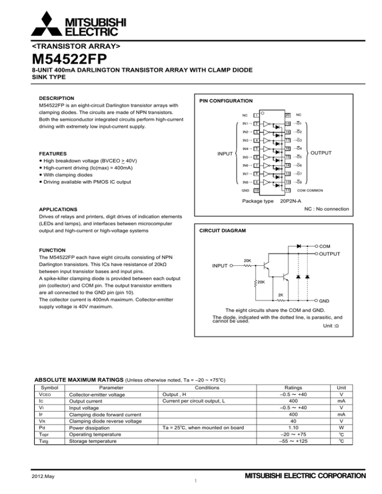
The M54522FP each have eight circuits consisting of NPN
20K
Darlington transistors. This ICs have resistance of 20kΩ
INPUT
between input transistor bases and input pins.
A spike-killer clamping diode is provided between each output
20K
pin (collector) and COM pin. The output transistor emitters
are all connected to the GND pin (pin 10).
2K
The collector current is 400mA maximum. Collector-emitter
GND
supply voltage is 40V maximum.
The eight circuits share the COM and GND.
The diode, indicated with the dotted line, is parasitic, and
cannot be used.
Unit :Ω
ABSOLUTE MAXIMUM RATINGS (Unless otherwise noted, Ta = –20 ~ +75℃)
Symbol
VCEO
IC
VI
IF
VR
Pd
Topr
Tstg
2012.May
Parameter
Collector-emitter voltage
Output current
Input voltage
Clamping diode forward current
Clamping diode reverse voltage
Power dissipation
Operating temperature
Storage temperature
Conditions
Output , H
Current per circuit output, L
Ta = 25℃, when mounted on board
1
Ratings
–0.5 ~ +40
400
–0.5 ~ +40
400
40
1.10
–20 ~ +75
–55 ~ +125
Unit
V
mA
V
mA
V
W
℃
℃
<TRANSISTOR ARRAY>
M54522FP
8-UNIT 400mA DARLINGTON TRANSISTOR ARRAY WITH CLAMP DIODE
SINK TYPE
RECOMMENDED OPERATING (Unless otherwise noted, Ta = –20 ~ +75℃)
Symbol
VO
Parameter
Output voltage
Collector current (Current per 1
circuit when 8 circuits are
coming on simultaneously)
IC
VIH
“H” input voltage
VIL
“L” input voltage
min
0
Limits
typ
-
max
40
0
-
400
0
-
200
8
4
0
-
-
Duty Cycle
no more than 5%
Duty Cycle
no more than 20%
IC < 400mA
IC < 200mA
Unit
V
mA
30
V
0.5
V
ELECTRICAL CHARACTERISTICS (Unless otherwise noted, Ta = -20~+75℃)
Symbol
Parameter
V (BR)CEO
VCE(sat)
Collector-emitter
breakdown voltage
Collector-emitter saturation
voltage
Input current
Clamping diode forward
voltage
Clamping diode reverse
current
DC amplification factor
II
VF
IR
hFE
Test conditions
min
Limits
typ *
Unit
max
V
ICEO = 100μA
40
—
—
VI = 8V, IC = 400mA
VI = 4V, IC = 200mA
VI = 17V
—
—
0.3
1.15
0.95
0.85
2.4
1.6
1.8
mA
IF = 400mA
—
1.5
2.4
V
VR = 40V
—
—
100
μA
1000
8000
—
—
VCE = 4V, IC = 300mA, Ta = 25℃
V
*:The typical values are those measured under ambient temperature (Ta) of 25℃.
There is no guarantee that these values are obtained under any conditions.
SWITCHING CHARACTERISTICS (Unless otherwise noted, Ta = 25℃)
Symbol
ton
toff
Parameter
Turn-on time
Turn-off time
Test conditions
min
—
—
CL = 15pF(note 1)
Limits
typ
30
930
Unit
max
—
—
ns
ns
TIMING DIAGRAM
NOTE 1 TEST CIRCUIT
INPUT
VO
INPUT
RL
Measured device
50%
50%
OPEN
OUTPUT
PG
50Ω
OUTPUT
CL
50%
ton
(1) Pulse generator (PG) characteristics: PRR = 1kHz,
tw = 10μs, tr = 6ns, tf = 6ns, ZO = 50Ω ,VI N= 0 to 8V
(2) Input-output conditions : RL = 25Ω, VO = 10V
(3) Electrostatic capacity CL includes floating capacitance at
connections and input capacitance at probes
2012.May
2
50%
toff
<TRANSISTOR ARRAY>
M54522FP
8-UNIT 400mA DARLINGTON TRANSISTOR ARRAY WITH CLAMP DIODE
SINK TYPE
TYPICAL CHARACTERISTICS
Output Saturation Voltage
Thermal Derating Factor Characteristics
Collector Current Characteristics
500
2.0
IC(mA)
1.5
Collector current
Power dissipation
Pd(W)
VI=4V
1.0
0.5
0
300
Ta=75℃
200
Ta=25℃
Ta=-20℃
100
0
0
25
50
75
Ambient temperature
100
0
Ta(℃)
0.5
1.0
1.5
Collector saturation voltage
Duty-Cycle- Collector current Characteristics
2.0
VCE(sat)(V)
Duty-Cycle- Collector current Characteristics
500
500
Collector current IC (mA)
Collector current IC (mA)
400
①
400
300
②
③
④
⑤
⑥
⑦
⑧
200
•The collector current values
represent the current per circuit.
•Repeated frequency ≥10Hz
•The value in the circle represents the
value of the simultaneously-operated circuit.
•Ta = 25℃
100
0
0
20
40
60
400
①
300
②
200
100
0
80
100
③
④
⑤⑥
⑦
⑧
•The collector current values
represent the current per circuit.
•Repeated frequency ≥10Hz
•The value in the circle represents the
value of the simultaneously-operated circuit.
•Ta = 75℃
0
20
40
60
80
100
Duty cycle (%)
Duty cycle (%)
DC Amplification Factor
Collector Current Characteristics
Grounded Emitter Transfer Characteristics
7
5
400
VCE=4V
VCE=4V
Collector current IC (mA)
DC amplification factor hFE
10 5
3
2
10
4
7
5
Ta=75℃
3
2
10
Ta=25℃
3
7
5
Ta=-20℃
3
300
Ta=75℃
Ta=25℃
Ta=-20℃
200
100
2
10
0
2
10 0
2
3
5 7
10 1 2 3
5 7
10 2 2 3
5 7
10 3
1
2
3
Input voltage VI (V)
Collector current IC (mA)
2012.May
0
3
4
<TRANSISTOR ARRAY>
M54522FP
8-UNIT 400mA DARLINGTON TRANSISTOR ARRAY WITH CLAMP DIODE
SINK TYPE
Clamping Diode Characteristics
Input Characteristics
400
Forward bias current IF (mA)
Input current II (mA)
2.0
1.5
Ta=-20℃
1.0
Ta=25℃
0.5
0
Ta=75℃
0
5
10
15
20
200
Ta=25℃
100
Ta=75℃
0
25
Input voltage VI (V)
2012.May
300
0
0.5
Ta=-20℃
1.0
1.5
Forward bias voltage VF (V)
4
2.0
<TRANSISTOR ARRAY>
M54522FP
8-UNIT 400mA DARLINGTON TRANSISTOR ARRAY WITH CLAMP DIODE
SINK TYPE
PACKAGE OUTLINE
2012.May
5
<TRANSISTOR ARRAY>
M54522FP
8-UNIT 400mA DARLINGTON TRANSISTOR ARRAY WITH CLAMP DIODE
SINK TYPE
Keep safety first in your circuit designs!
Mitsubishi Electric Corporation puts the maximum effort into making semiconductor products better and more
reliable, but there is always the possibility that trouble may occur with them. Trouble with semiconductors
may lead to personal injury, fire or property damage. Remember to give due consideration to safety when
making your circuit designs, with appropriate measures such as (i) placement of substitutive, auxiliary
circuits, (ii) use of non-flammable material or (iii) prevention against any malfunction or mishap.
Notes regarding these materials
•These materials are intended as a reference to assist our customers in the selection of the Mitsubishi
semiconductor product best suited to the customer’s application; they do not convey any license under
any intellectual property rights, or any other rights, belonging to Mitsubishi Electric Corporation or a third
party.
•Mitsubishi Electric Corporation assumes no responsibility for any damage, or infringement of any thirdparty’s rights, originating in the use of any product data, diagrams, charts, programs, algorithms, or
circuit application examples contained in these materials.
•All information contained in these materials, including product data, diagrams, charts, programs and
algorithms represents information on products at the time of publication of these materials, and are
subject to change by Mitsubishi Electric Corporation without notice due to product improvements or
other reasons. It is therefore recommended that customers contact Mitsubishi Electric Corporation or an
authorized Mitsubishi Semiconductor product distributor for the latest product information before
purchasing a product listed herein.
The information described here may contain technical inaccuracies or typographical errors. Mitsubishi
Electric Corporation assumes no responsibility for any damage, liability, or other loss rising from these
inaccuracies or errors.
Please also pay attention to information published by Mitsubishi Electric Corporation by various means,
including the Mitsubishi Semiconductor home page (http://www.MitsubishiElectric.com/).
•When using any or all of the information contained in these materials, including product data, diagrams,
charts, programs, and algorithms, please be sure to evaluate all information as a total system before
making a final decision on the applicability of the information and products. Mitsubishi Electric
Corporation assumes no responsibility for any damage, liability or other loss resulting from the
information contained herein.
•Mitsubishi Electric Corporation semiconductors are not designed or manufactured for use in a device or
system that is used under circumstances in which human life is potentially at stake. Please contact
Mitsubishi Electric Corporation or an authorized Mitsubishi Semiconductor product distributor when
considering the use of a product contained herein for any specific purposes, such as apparatus or
systems for transportation, vehicular, medical, aerospace, nuclear, or undersea repeater use.
•The prior written approval of Mitsubishi Electric Corporation is necessary to reprint or reproduce in
whole or in part these materials.
•If these products or technologies are subject to the Japanese export control restrictions, they must be
exported under a license from the Japanese government and cannot be imported into a country other
than the approved destination.
Any diversion or re-export contrary to the export control laws and regulations of Japan and/or the
country of destination is prohibited.
•Please contact Mitsubishi Electric Corporation or an authorized Mitsubishi Semiconductor product
distributor for further details on these materials or the products contained therein.
© 2012 MITSUBISHI ELECTRIC CORPORATION. ALL RIGHTS RESERVED.
2012.May
6
