FPGA I/O – When To Go Serial
Page 1 of 8
HOME :: FPGA ENCYCLOPEDIA :: ARCHIVES :: MEDIA KIT :: SUBSCRIBE
Ads by Google
FPGA I/O – When To Go Serial
by Brock J. LaMeres, Agilent Technologies
Physical
Synthesis Tools
Learn How to Solve
Timing Closure
Problems Fast Free Tech Papers
www.mentor.com/fpga
Fpga Synthesis
High Performance,
low cost solution
Free Software,
Workshops &
More!
www.xilinx.com/design
Over the past decade, FPGAs have gained a foothold as one of the most used
building blocks in digital systems. The flexibility of an FPGA allows designers to
decrease hardware design cycles while adding inherent feature upgradability in the final product. In
Free Quartus II
Software
Support New
Cyclone II FPGA
Design. Request a
Free Copy from
Altera Now
www.altera.com
addition, the data rates of modern FPGAs are competing with CMOS ASICs, thus allowing the
needed system performance to be achieved using what was once only a proto-typing vehicle.
The data rates of modern FPGAs are giving designers the freedom to create their own application
specific busses. However, designers are quickly learning the pitfalls of running I/O at high speeds.
Factors such as channel-to-channel skew, jitter, and aperture window size are limiting the
theoretical data rates of the FPGAs specifications. To address these issues, FPGA system designers
Get Free DSP
Newsletter
Learn about
Altera's Digital
Signal Processing
Solutions.
Subscribe Now
www.altera.com
are following suit to their ASIC predecessors and adopting I/O architectures that inherently reduce
the effect of the above-mentioned factors.
This article will present the most popular I/O architectures in use today. In addition, the factors that degrade the
performance of the I/O will be discussed for each architecture. Finally, a guide for selecting the appropriate I/O
architecture for the application will be presented.
FPGA I/O – When To Go Serial
Page 2 of 8
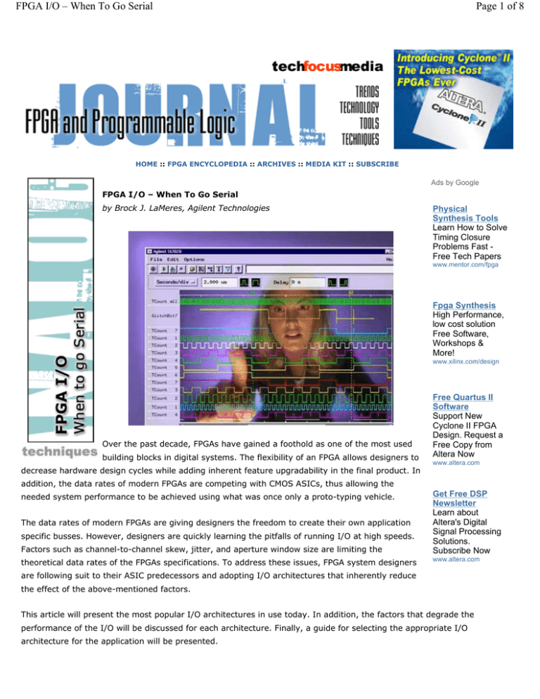
Figure 1. Modern digital systems are using FPGAs due to their flexibility and speed.
Designers are facing the pitfalls of running I/O at high speeds.
I/O CLOCKING ARCHITECTURES
Synchronous Clocking
Synchronous clocking is the most widely used clocking scheme in digital systems. In this type of clocking, there is one
clock that is distributed to all synchronous logic in the system. All transactions occur at a particular edge of this one clock.
This type of clocking has the advantage that it is relatively simple to implement. However, in order to ensure timing
accuracy, the clock distribution network must be matched in electrical length to all of the synchronous logic in the system.
This becomes increasingly difficult when clock paths enter FPGAs with complex logic and connect multiple FPGAs that are
created with various processes and different packaging. The variation in IC process and construction leads to timing error
that degrades the performance of this type of clocking. Another limitation is that after a clocking event, the next clock
must wait until the data has successfully traveled from one FPGA to the other. Examples of this type of architecture are
the Pentium I uP, the PCI bus, and SDRAM memory.
Source Synchronous Clocking
Source Synchronous Clocking was developed to address the difficulty that synchronous clocking has with matching the
clock distribution paths to each element in the system. In this type of clocking, the circuit that is producing the data
pattern will create its own clock that is transferred along with the data. Generating the clock in the same geographical
location as the data in addition to having the clock traverse the same media as the data bus creates a much tighter timing
correlation. The tighter timing means that the data valid windows of the data being latched are better aligned with the
clock used to latch them. This reduced channel-to-channel skew allows data transfer rates to exceed that of a
synchronous architecture. Examples of this type of architecture are Intel’s IA32 front side bus and DDR memory.
Embedded Clocking
Source synchronous clocking is prone to the same channel-to-channel skew as synchronous timing, albeit at a much
higher data rate. The difference in process variation and interconnect structure between channels within an FPGA will
FPGA I/O – When To Go Serial
Page 3 of 8
contribute to channel-to-channel skew no matter how tightly the clock is coupled to the multiple signals. To address this
problem, embedded clocking was invented. In embedded clocking, the data is encoded in a manner that will guarantee a
certain number of transitions per time (i.e., 8B/10B encoding). By ensuring that the data will transition a certain
percentage of unit time, a PLL can then lock to the data stream. In embedded clocking, a PLL is used at the receiver that
will lock onto the incoming data stream and create a clock based off of the transition frequency. This clock is then
centered within the data valid window. The drawback of this type of clocking is that the clock centering is only valid for
the data channel to which the PLL has locked. However, the data rate for an individual channel is only limited by its jitter
margin and aperture window. This type of clocking can achieve extremely high data rates (> 2.5Gb/s) relative to
synchronous and source synchronous designs. This type of design requires more complex circuitry at both the driver and
receiver but the data rates achieved are so much higher than previous architectures that the channel counts can be
reduced while still delivering an overall throughput increase.
Figure 2. FPGA Designers are changing their I/O architectures to overcome the signal integrity
issues that arise when running at fast data rates.
FACTORS IN SELECTING AN I/O ARCHITECTURE
The total throughput (or digital bandwidth) is defined as the number of symbols that can be transmitted per second. This
depends on the Unit Interval that can be achieved per channel and the number of channels used in to the I/O
architecture.
Channel-to-Channel Skew
Channel-to-channel skew refers to the time difference of the data valid windows between various signal paths. This issue
FPGA I/O – When To Go Serial
Page 4 of 8
is due to electrical length differences in the physical signal paths. These paths vary for each channel due to the
implementation of the circuit.
The skew between channels will limit the data rate of the I/O architecture. This is because the synchronizing clock for the
data signals must be placed such that it can successfully latch in all of the data channels in the bus. To achieve this
placement, the net data valid window of all of the overlaid channels must be large enough for the clock to be placed
within. The more channels that are used increase the chance for channel-to-channel skew. As more channels are used,
the net data valid window will decrease thus reducing the maximum transfer rate.
There are two main sources of skew. The first is the electrical length mismatch on the IC. The majority of this mismatch
comes from the packaging interconnect. When using an FPGA, the complex logic can also be a major factor. As CMOS dies
approach sizes of 20mmX20mm and packages reach signal counts into the thousands, the difference in channel path
length becomes considerable. The on-chip skew is also exacerbated by the fact that signals are being driven from one
large FPGA package to another. This can effectively double the skew due to on-chip path length.
The second source of skew is due to channel mismatch on the PCB. This skew is due to either a physical mismatch of PCB
traces on the same layer or a propagation delay mismatch of PCB traces on different layers. The following figure shows an
example of channel-to-channel skew.
Figure 3. Tools such as logic analyzers can give designers an in-sight into the net channel-tochannel skew that the FPGAs are experiencing. This measurement was taken using a tool called “Eye
Finder” from Agilent Technologies, Inc. Note the data valid window size shrinkage when all of the
signals in the bus are overlaid.
FPGA I/O – When To Go Serial
Page 5 of 8
Jitter
Jitter is a term that describes the timing uncertainty within a Unit Interval. Said otherwise, jitter is the amount of time
within a UI in which it cannot be guaranteed that the data is at a stable logic level. This uncertainty region will limit how
small of a UI can be used while still transmitting reliable data. The two major subsets of Jitter are deterministic and nondeterministic jitter.
Deterministic Jitter
Deterministic jitter refers to sources of jitter that can be calculated. For example, if a product is specified to operate with
5% power supply variation, then the timing uncertainty due to supply drop needs to be considered in the data rate
specification. While how much timing uncertainly will vary from application to application, the entire range of timing
uncertainty must be accounted for. Some possible sources of deterministic jitter can be process variation, ISI, reflections,
simultaneous switching noise, power supply droop, and RC load variation. These sources can all be quantified in the
design and added to a timing uncertainly stackup. The worst-case impact of each of these sources must be accounted for
in a stable design.
Non-Deterministic Jitter
Non-deterministic jitter refers to statistical sources of timing uncertainty. These are sources in which the noise
contribution is modeled by their probability distribution rather than their worst-case value. Traditionally these sources are
modeled using a Gaussian distribution. The figures-of-merit for these sources are their RMS value or standard deviation.
For these types of sources, the worst-case impact does not need to be accounted for since statistically it will happen
infrequently. Instead, a bit error rate is used to predict system stability. A few examples of these types of noise sources
are thermal and shot noise. Multiple sources of statistical noise are accounted for using an RMS summation to find the net
contribution of statistical noise.
Jitter can be very difficult to predict. Typically its contribution is found using jitter measurement techniques in an
oscilloscope. By allowing an acquisition to accumulate for a relatively large amount of time, the distribution of jitter can be
found. A note on this technique is that all of the sources of jitter are measured simultaneously. While this has the
drawback of not isolating individual sources, it is usually the only method available to FPGA designers.
FPGA I/O – When To Go Serial
Page 6 of 8
Figure 4. Jitter measurement taken on a 2.5Gb/s signal using a 54750A sampling oscilloscope. Note
the histogram used to find the jitter distribution.
Receiver Aperture Window
The final contribution to the speed of an I/O design is the aperture window of the receiving element. This is traditionally
called setup and hold but refers to the minimum time that the data must be stable before and after the timing event in
order for the receiver to capture the symbol. The aperture window must be able to fit within the net data valid window of
all of the overlaid data channels to ensure successful data collection. FPGA manufacturers will specify this value. However,
complex logic and data path variation will degrade the ideal specification. In most cases a measurement is needed.
Calculation of Throughput
The combination of channel-to-channel skew, jitter, and receiver aperture dictate how fast the I/O design can operate. We
define the channel-to-channel skew as the time difference between the transition regions of two channels when operating
in the same phase (i.e., intending to transmit a symbol at the same time). The following equations relate the total bit
transfer rate per channel to the sources of error described above.
SELECTING AN FPGA I/O ARCHITECTURE
The first step in selecting an I/O architecture is determining the design’s data throughput requirement. Once this is
defined, I/O architectures can be evaluated for selection. This is an interactive process requiring measurement data. All of
the factors, channel-to-channel skew, jitter, aperture window, will increase as signals are added to the I/O design. The
best way to find these contributions is through empirical data from oscilloscopes and logic analyzers.
FPGA I/O – When To Go Serial
Page 7 of 8
Starting with the simple synchronous architecture, signals can be added to increase the overall throughput. As signals are
added, the degradation factors must be observed. At some point, the addition of signals is no longer practical because of
the adverse signal integrity contributions, the main contribution being channel-to-channel skew.
At this point, the source synchronous architecture can be explored. The major advantage of this architecture is that it
dramatically reduces the channel-to-channel skew within a data group. At some point the channel-to-channel skew will
again become an issue, but at a much higher data rate. The skew in this architecture will be on the same order of
magnitude as the jitter contribution.
Finally, the embedded clock architecture can be examined. This architecture has the advantage in that there is no
channel-to-channel skew due to the clock/data recovery design. In addition, the jitter is reduced because there is no
longer a data channel and a clock channel that possess jitter. This architecture will be limited only by the jitter and
aperture window contribution.
If industry I/O standards are observed, they typically fall into the following table of data rates.
Individual Channel Data Rate
Clocking Scheme
DC – 300 Mb/s
Synchronous
300 Mb/s - 2Gb/s
Source Synchronous
> 2G/bs
Embedded Clock
Table 1.
Per channel data rates observed in industry for the clocking architectures presented.
This illustrates the evolution of I/O architecture of both ASICs and in FPGAs.
CONCLUSION
As FPGA speeds have increased over the past decade, designers are using FPGAs as an alternative to ASICs. However,
designers are quickly discovering that the increased FPGA speeds are leading to the same signal integrity problems that
ASIC designers have been facing for years. As signals are added to an I/O architecture to increase the total throughput,
the channel-to-channel skew, jitter, and aperture window contributions are increased. To address these problems, FPGA
designers must turn to different clocking architectures. In order to maintain the trend of increased system data rates, a
designer using FPGAs must first understand all of the contributions to the unit interval reduction in order to be successful.
Brock J. LaMeres, Agilent Technologies
August 3, 2004
--------------------------------------------------About the Author: Brock LaMeres received his B.S.E.E. from Montana State University and his M.S.E.E. from the
University of Colorado. He is currently a hardware design engineer for Agilent Technologies, where he designs high-speed
printed circuit boards used in logic analyzers. He is also a part-time instructor in microprocessor systems at the University
of Colorado in Colorado Springs. His research interests include modeling and characterization of transport systems and
high-speed digital design.
[back to top]
FPGA I/O – When To Go Serial
Comments on this article? Send them to comments@fpgajournal.com
All material on this site copyright © 2003-2004 techfocus media, inc. All rights reserved.
Page 8 of 8
