Boise State University Digital Systems Laboratory Electrical and Computer Engineering Department ECE230L
advertisement
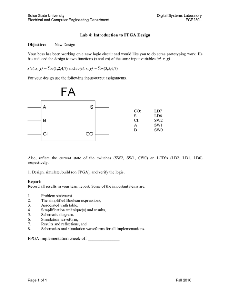
Boise State University Electrical and Computer Engineering Department Digital Systems Laboratory ECE230L Lab 4: Introduction to FPGA Design Objective: New Design Your boss has been working on a new logic circuit and would like you to do some prototyping work. He has reduced the design to two functions (s and co) of the same input variables (ci, x, y). s(ci, x, y) = m(1,2,4,7) and co(ci, x, y) = m(3,5,6,7) For your design use the following input/output assignments. CO: S: CI: A B LD7 LD6 SW2 SW1 SW0 Also, reflect the current state of the switches (SW2, SW1, SW0) on LED’s (LD2, LD1, LD0) respectively. 1. Design, simulate, build (on FPGA), and verify the logic. Report: Record all results in your team report. Some of the important items are: 1. 2. 3. 4. 5. 6. 7. 8. Problem statement The simplified Boolean expressions, Associated truth table, Simplification technique(s) and results, Schematic diagram, Simulation waveform, Results and reflections, and Schematics and simulation waveforms for all implementations. FPGA implementation check-off ______________ Page 1 of 1 Fall 2010

