Bonding in Metals and Semiconductors
advertisement
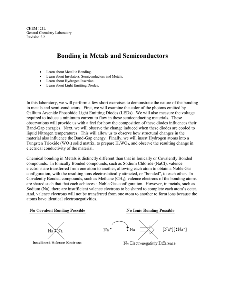
CHEM 121L General Chemistry Laboratory Revision 2.2 Bonding in Metals and Semiconductors Learn about Metallic Bonding. Learn about Insulators, Semiconductors and Metals. Learn about Hydrogen Insertion. Learn about Light Emitting Diodes. In this laboratory, we will perform a few short exercises to demonstrate the nature of the bonding in metals and semi-conductors. First, we will examine the color of the photons emitted by Gallium Arsenide Phosphide Light Emitting Diodes (LEDs). We will also measure the voltage required to induce a minimum current to flow in these semiconducting materials. These observations will provide us with a feel for how the composition of these diodes influences their Band-Gap energies. Next, we will observe the change induced when these diodes are cooled to liquid Nitrogen temperatures. This will allow us to observe how structural changes in the material also influence the Band-Gap energy. Finally, we will insert Hydrogen atoms into a Tungsten Trioxide (WO3) solid matrix, to prepare HxWO3, and observe the resulting change in electrical conductivity of the material. Chemical bonding in Metals is distinctly different than that in Ionically or Covalently Bonded compounds. In Ionically Bonded compounds, such as Sodium Chloride (NaCl), valence electrons are transferred from one atom to another, allowing each atom to obtain a Noble Gas configuration, with the resulting ions electrostatically attracted, or “bonded”, to each other. In Covalently Bonded compounds, such as Methane (CH4), valence electrons of the bonding atoms are shared such that that each achieves a Noble Gas configuration. However, in metals, such as Sodium (Na), there are insufficient valence electrons to be shared to complete each atom’s octet. And, valence electrons will not be transferred from one atom to another to form ions because the atoms have identical electronegativities. P age |2 Instead, the bonding is collective; each atom contributes its valence electrons to form a “sea” of electrons which are shared by all the atoms of the metal. The resulting metal cation cores are held together by their attraction to this “sea” of delocalized electrons. For a concrete example, consider the bonding between two Sodium atoms that form the hypothetical Na2 molecule. Each atom involved in the bonding has the following electron configuration: Na = 1s2 2s2 2p6 3s1 = [Ne] 3s1 Thus, each Na atom has a single valence electron in the 3s orbital. When the two Na atoms approach each other, the 3s valence level orbitals will overlap, creating a region of high electron density where the two valence electrons can be shared by both atoms. The resulting “Molecular Orbital” gives rise to an energetically favorable configuration and is referred to as a Bonding MO. P age |3 However, this picture is a bit simplistic. We have to admit that orbitals are merely representations of Wavefunctions, mathematical waves, which, like other wave pulses, can have a positive or negative Amplitude. If two wave pulses of positive amplitude interact, they will constructively interfere: However, if the pulses are of opposite amplitude, the interference will be destructive: If the two pulses are of equal shape and amplitude, a nodal plane, a surface of zero amplitude, will occur when their interference is maximal. Likewise, interaction of Atomic Orbitals, such as the 3s orbitals of our Sodium atoms, can be between orbitals of similar amplitude, which will lead to constructive interference, or between orbitals of opposite amplitude, giving rise to destructive interference. P age |4 As noted above, constructive interference produces a bonding Molecular Orbital. However, destructive interference gives rise to a region of low electron density between the atoms; an energetically unfavorable configuration which is an anti-bonding Molecular Orbital. Once the Molecular Orbitals have been formed, they must be populated with valence electrons. In our case, each Na atom brings with it a single 3s valence electron. Hence, the Na2 molecule will have 2 valence electrons in these Molecular Orbitals. The electrons will occupy the lowest energy orbital possible according to the Principle of Pauli and the Rule of Hund. P age |5 For Na2, both electrons will fill the Bonding MO with spins antiparallel. The Anti-Bonding MO will remain unoccupied. We refer to the MO of highest energy which is occupied as the Highest Occupied Molecular Orbital ,or HOMO. The Lowest Unoccupied Molecular Orbital is the LUMO. It must be kept in mind, we have only considered the formation of MO’s from the valence level orbitals (3s) of the Na atom. MO’s will also form from core level orbitals; 1s, 2s and 2p. These MO’s will all be completely filled. Likewise, MO’s can also be formed from atomic orbitals beyond the valence shell; 3p, 3d, 4s, 4p, etc. These MO’s will all be unfilled. If a cluster of 4 Sodium atoms now attempts to bond to form Na4, 4 atomic orbitals (3s) will combine to form 4 molecular obitals (MO). The exact energies of the resulting MOs will depend on the geometric configuration of the cluster. In general, however, the result will be two closely spaced bonding MO’s and two closely spaced anti-bonding MO’s. (The total number of MO’s, bonding and anti-bonding, will equal the total number of atomic orbitals used to form the MO’s.) So, for the case of Na4, we have an energy diagram that appears as: The 4 valence electrons will fill the 2 Bonding MO’s; with the higher of these being the HOMO. The LUMO will be the lowest lying Anti-Bonding MO. If we include other valence level orbitals (3p) and move to large numbers of bonding atoms (Avogadro’s Number), the resulting MOs will form an energy continuum. P age |6 The low lying orbitals will be occupied with valence level electrons and form a Valence Band. Unoccupied, higher energy orbitals make-up the metal’s Conduction band. The “sea” of electrons which comprise the collective Valence Band give rise to bonding in the metal. However, with very little energy electrons can be promoted from the Valence Band to the Conduction Band and they become free to migrate, allowing for the observed electrical conductivity of the metal. (Why are the HOMO and LUMO not located in the middle of the diagram, with an equal number of filled and unfilled MO’s below and above them?) This “band” picture can be extended to other networked solids such as Diamond (C) or semiconductors such as Germanium (Ge). In the former case, the electrons are localized in C-C bonds. This localization of the electrons in specific bonds gives rise to tighter and stronger bonds between the atoms. This means the bonding MOs will separate from the antibonding MOs by a larger energy gap, giving rise to a “Band-Gap” between the Valence and Conduction bands. This makes it harder to promote electrons into the Conduction band, making the material an insulator. Semi-conducting materials lie between the extremes of localized and delocalized bonding, resulting in a small Band-Gap. If the orbitals involved in forming the MOs are smaller, overlap between them is greater, and the bonding is tighter. This has the effect of increasing the Band-Gap. Thus, Diamond (C) is an insulator whereas Silicon and Germanium are semiconductors. -Tin, with very large atoms, is a metal. This, in spite of the fact that all are from the same Chemical Group; Group 4A. P age |7 Likewise, the strength with which an electron is held in a localized bond is increased with an increasing electronegativity difference between the atoms involved in the bonding. Thus, the Band-Gap increases for the following series: Ge < GaAs < ZnSe < CuBr even though the Unit Cell size is similar for each of these compounds. In this laboratory we will examine semiconducting materials that have a Diamond-like structure. Recall, Carbon (C) has four valence electrons; thus, in diamond each Carbon atom will be bonded to four other Carbon atoms in a tetrahedral network; a unit cell of which is pictured below. As noted above, Diamond has highly localized bonds and is thus a good insulator. We can form semiconducting materials that have a similar structure by mixing Gallium (Ga), which has 3 valence electrons, with either Phosphorus (P) or Arsenic (As), each having 5 valence electrons. This gives us, on average, four valence electrons per atom, similar to the four valence electrons per Carbon (C) in Diamond. P age |8 Gallium Arsenide Phosphide materials are available commercially as solid solutions with the non-stoichiometric formula: GaPxAs1-x 0 < x <1 and are fabricated as LEDs. Here, x represents a sliding scale between two extremes, GaP and GaAs. Between these extremes, the percentage of Phosphorus and Arsenic, per Gallium atom, will vary. Because the composition of these materials is not fixed, like H2O, which is always 2 Hydrogen atoms per Oxygen atom, they are not considered compounds in the traditional sense. They are instead solid solutions; more akin to Salt-Water solutions where the percentage Salt can vary from 0% to 35% by weight. Very crudely, this might be as pictured: By varying the amount of Phosphorus and Arsenic in the solid solution, we can tune the BandGap energy to any desired value. In the LED, electrons are excited into the Conduction Band by harnessing the chemical energy of a 9 Volt battery. When the electrons return to the Valence Band, the excess energy is emitted as a photon. P age |9 The wavelength () of the photon is related to its speed (c) via: c = (Eq. 1) where is its frequency. In a vacuum the speed of a photon is c = 2.99792 x 10⁸ m/sec. Its energy (E) is then related to its frequency via: E = h (Eq. 2) where h represents Planck’s constant; h = 6.62608 x 10⁻³⁴ Jsec. Thus, the color of the photon emitted will give us an estimate of the Band-Gap for the semiconductor because: Band-Gap ~ Ephoton = hc / (Eq. 3) (For a variety of reasons we will not discuss, this is not an exact relationship.) We will also measure the Voltage required to kick electrons into the Conduction Band, which will also be proportional to the Band-Gap. Then, we will cool the LEDs to liquid Nitrogen temperatures and see what effect the resulting structural changes have on the Band-Gap. P a g e | 10 Finally we will reductively insert Hydrogen (H) atoms into a Tungsten Oxide (WO3) matrix. WO3 + (x/2) H2 HxWO3 (Eq. 4) forming another type of solid solution. These Hydrogen atoms are generated by the Reduction of Hydrochloric Acid (HCl): 2 HCl(aq) + Zn(s) H2(g) + ZnCl2(aq) (Eq. 5) Each Hydrogen atom inserted into the WO3 matrix brings a single electron with it. These electrons will be donated to the material’s Conduction Band and cause the material to act like a metal. This will manifest itself in a measurable change in the electrical conductivity of the material. P a g e | 11 Pre-Lab Safety Questions 1. What is the OSHA regulatory statement concerning "face velocity" of air flow for safety fume hoods? 2. What is the ANSI regulatory statement concerning "face velocity" of air flow for safety fume hoods? 3. Consult an SDS for Tungsten Trioxide. What is the "Time Weighted Average" exposure limit for this substance? For our purposes, will we need to use the Tungsten Trioxide in a fume hood? 4. What is the suggested method for treating an "inhalation exposure" to Tungsten Trioxide? P a g e | 12 Procedure Hydrogen Insertion into WO3 1. Place 0.5g of Tungsten Trioxide (WO3) into a 150 mL beaker. Caution: WO3 is an irritant. Avoid creating or breathing dust from this compound. Avoid eye and skin contact. Wash your hands thoroughly after handling. Note the color of the compound. 2. Carefully pour about 50 mL of 3M Hydrochloric Acid (HCl) onto the WO3. Observe the results. 3. Add less than 0.6g of Zinc (Zn) fillings to the Acid, stir briefly with a stirring rod and observe what takes place. 4. After the reaction has ceased, note the colors of all the products. Filter off, using a Buchner funnel, the solid product. Wash the product twice with Water and air dry for a few minutes. Your product must be thoroughly dry for the conductivity measurements. 5. Test the conductivity of your product and the Tungsten Trioxide starting material. Weigh out separately, on glazed weighing paper, about 0.15g of both the product and starting material. Obtain a Teflon plug fitted with two brass thumb screws. Using a small spatula, and with one brass screw in place, fill the plug with the weighed product. Scrape any excess off the end of the plug. Insert the other brass thumb screw and tighten until "finger tight." P a g e | 13 Using an Ohmmeter (10-100 k range) measure the electrical resistance of the sample. Do the same for the Tungsten Oxide starting material. 8. Test for the reversibility of the Hydrogen insertion by placing your product on a small watch glass that has been labeled with your name. Place the watch glass in an oven at 100oC for 90 minutes. Note any changes that occur over this period time. Color vs. Composition of LEDs 1. Build the following circuit: One group should build the circuit using a 1 k resistor, and a neighboring group should do the same using a 1 M resistor. Each connection should be made by soldering the two leads to each other. Soldering is usually easier if you melt some solder onto each lead individually before trying to join them together. A wooden spring clothespin is a convenient way to hold the socket while soldering. P a g e | 14 2. Obtain four samples of the four different GaPxAs1-x LEDs. Using the circuit containing the 1 k resistor, connect the battery snap to a 9 V battery. Insert an LED into the circuit. Record the color emitted. Repeat for each of the four LEDs. (Does it matter which way the LED is inserted?) 3. When a voltage is applied across the LED, nothing happens unless the energy, which is proportional to the voltage, is sufficient to excite an electron into the conduction band. When the energy is increased beyond the band-gap energy, current can begin to flow. Measurement of the voltage for a minimum current flow provides another estimate of the band-gap energy. To approximate the conditions of minimum current flow, use the circuit containing the 1 M resistor. Insert an LED into the circuit. Measure the voltage across the LED. (If the voltage is more than 3 V, then current is not flowing through the LED and its electrical leads should be reversed.) (The data obtained will not represent the actual band-gap energies, because thermal excitation of localized electrons contributes to the current, but the trend will be correct.) Diffraction of White Light 1. Obtain a White LED and plug it into your circuit containing the 1 k resistor. 2. View it through a diffraction grating. 3. Make particular note as to which region of the Visible Spectrum is dispersed the greatest and which the least. Temperature Effects for LEDs 1. Working with another group, use two circuits containing 1 k resistors and GaP0.40As0.6 LEDs inserted. Practice holding the LEDs in a column and viewing the spectral lines through a Diffraction Grating. The dispersion of the spectral lines should be the same for both diodes. 2. Dip only one lighted LED into a dewar filled with liquid Nitrogen. Caution: Do not allow the liquid Nitrogen to come into contact with your skin. Allow the LED to cool for a few seconds. 3. Then, view, through the Diffraction Grating, the cold LED, with the Room Temperature LED as a reference. Make particular note of the dispersion of the light emitted by the “cold” vs. the “warm” LED. P a g e | 15 4. Repeat this procedure using GaP0.65As0.45 LEDs. Temperature Effects for Metals 1. Obtain a copper RF Coil. This will be our “metal” sample in determining the temperature dependence of the Resistance in metals. Resistance measures the difficulty with which an electron moves through a material. 2. Use a digital voltmeter on the resistance setting (200) to record the resistance of the Coil. 3. Dip the Coil into liquid Nitrogen. Make note of the change in resistance. This procedure was adapted from Teaching General Chemistry: A Materials Science Companion by Arthur B. Ellis, Margaret J. Geselbracht, Brian J. Johnson, George C. Lisensky, and William R. Robinson; American Chemical Society, 1993. P a g e | 16 Data Analysis Color vs. Composition of LEDs 1. Prepare a list of LED composition (GaPxAs1-x), from smallest to largest x versus Color and Min. Current LED Voltage. 2. Considering only Atomic Radii, rank the following in order of increasing band-gap energy: GaP0.40As0.60, GaP0.65As0.35, GaP0.85As0.15, GaP1.00As0.00 Is your prediction consistent with your observations? Explain. 3. Considering only Electronegativity, rank the following in order of increasing band-gap energy: GaP0.40As0.60, GaP0.65As0.35, GaP0.85As0.15, GaP1.00As0.00 Is your prediction consistent with your observations? Explain. 4. Are the Color and Voltage trends consistent with your predictions? Explain. Temperature Effects for LEDs 1. What do you expect to happen to bond distances in materials as they are cooled? Explain. What effect will this have upon the band-gap energy of the material? 2. Did the wavelength of the light emitted from the cold LEDs change? If so, to higher or lower photon energy? 3. Is your prediction consistent with your observation? Explain. Temperature Effects for Metals 1. The Conductivity of metals decreases with increasing Temperature. However, the Conductivity of semi-conductors increases. Explain these two trends. 2. Are your observations consistent with the above statement? Explain. P a g e | 17 Hydrogen Insertion into WO3 1. Has the conductivity of the HxWO3 changed when compared with WO3? If so, is the change consistent with your expectations? Explain. P a g e | 18 Post Lab Questions 1. The Band structures of metallic Sodium (Na) and Magnesium (Mg) are constructed from 3s and 3p orbitals and can be pictured roughly as: Sketch, roughly, how this Band structure will fill with valence electrons for the Sodium (Na) and Magnesium (Mg) cases. 2. How can metallic luster be explained by the theory of metallic bonding? (Hint: Consider the wavelength of the photons that can be absorbed by the metal, and those that can be emitted.)
