ISSN 2319-8885
Vol.04,Issue.39,
September-2015,
Pages:8550-8557
www.ijsetr.com
Single Stage Boost Inverter with PV Input
E. GANESH KUMAR1, P. KAMALAKAR2
1
PG Scholar, Dept of EEE, Malla Reddy Engineering College, Maisammaguda, Dhulapally, Telangana, India.
Associate Professor, Dept of EEE, Malla Reddy Engineering College, Maisammaguda, Dhulapally, Telangana, India.
2
Abstract: This paper is to study the operating modes and analysis of the Switched Boost Inverter (SBI). The performance of the
proposed SBI is similar to that of Z-Source Inverter (ZSI). This SBI converter can possible to supply both DC and AC loads
simultaneously from a single dc input source. Here, reducing the inverter switching stress. Also, this converter provides to shootthrough of the inverter legs without causing any damage to the inverter switches. The unique feature of the SBI, it can operate
boost mode operations with a wide range of obtainable output voltages from a given input voltage.SBI construct similar
advantages of converter uses more switching devices and lower number of passive devices compared to the original ZSI. Along
with its pulse width modulation (PWM) control strategies is give the inverter switching pulse. Fuzzy Logic Controller to control a
switch of a Boost Converter. In order to increase the efficiency of the energy conversion for the system using a resonant switching
technique. The simulations results are obtained by MATLAB/SIMULINK software.
Keywords: Pulse Width Modulation (PWM), Voltage Source Inverter (VSI), Switched Boost Inverter.
I. INTRODUCTION
ZSI employs a unique impedance network to couple the
converter circuit to the power source, thus providing unique
characteristic features that cannot be found in the traditional
Voltage source inverter and Current source inverter. The
unique impedance network mentioned above, implements
two capacitors and two inductors. Introduction of these
passive components add weight and size to the whole
inverter. In order to reduce size and weight, a new topology
is considered which involves lesser passive components,
meanwhile trying to attempt similarity in all the steady state
performance. This new topology is called Switched Boost
inverter, which is being studied and analyzed in this report.
The Z-Source inverter is a new and attractive topology for
the power electronics interface. In recent Years, renewable
energy is becoming increasingly important in distribution
System, which provide different choice to electricity
consumers whether they receive power from the main
electricity source or in forming a micro source not only to
fulfill their own demand but alternatively to be a power
producer supplying a micro grid.
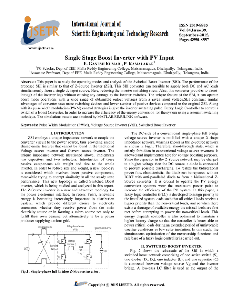
Fig.1. Single-phase full bridge Z-Source inverter.
The DC-side of a conventional single-phase full bridge
voltage source inverter is modified with a unique X-shape
impedance network, which is known as the Z-Source network
as shown in Fig.1. Therefore, shoot-through state, which is
strictly forbidden in conventional voltage source inverters, is
allowed and implemented here for voltage boosting purposes.
Since the capacitor in the Z-Source network may be charged
to a higher voltage than the DC source, a diode is connected
to prevent possible discharging. To realize the bidirectional
power flow characteristic, the diode can be replaced with an
IGBT with anti-paralleled diode to form a bidirectional ZSource converter. It is crucial to operate the PV energy
conversion systems wear the maximum power point to
increase the efficiency of the PV system. In this paper, a
fuzzy logic controller (FLC) is developed to assign priority to
the installed system loads such that all critical loads receive a
higher priority than the non-critical loads, and so when there
exists a shortage of available energy the critical loads are first
met before attempting to power the non-critical loads. This
energy dispatch controller is also optimized to maintain a
higher battery charge so that the controller is better able to
power critical loads during an extended period of unfavorable
weather conditions or low solar insulation. In this study, the
simultaneous optimization of the membership functions and
rule base of a fuzzy logic controller is carried out.
II. SWITCHED BOOST INVERTER
Fig. 2 shows the schematic of the SBI in which a
switched boost network comprising of one active switch (S),
two diodes (Da, Db), one inductor (L), and one capacitor (C)
is connected between voltage source Vg and the inverter
bridge. A low-pass LC filter is used at the output of the
Copyright @ 2015 IJSETR. All rights reserved.
E. GANESH KUMAR, P. KAMALAKAR
inverter bridge to filter the switching frequency components
The inverter bridge is represented by a current source in
in the inverter output voltage vAB. Similar to a ZSI, the SBI
this interval as shown in the equivalent circuit of Fig. 4 Now
also utilizes the shoot-through state of the H-bridge inverter
the voltage source Vg and inductor L together supply power
(both switches in one leg of the inverter are turned on
to the inverter and the capacitor through diodes Da and Db.
simultaneously) to boost the input voltage Vg to VC [10].
The inductor current in this interval equals the capacitor
charging current added to the inverter input current. Note that
the inductor current is assumed to be sufficient enough for
the continuous conduction of diodes Da and Db for the entire
interval (1 − D).TS [11].
III. PWM CONTROL OF SBI
The SBI utilizes the shoot-through state of VSI to boost
the input voltage Vg, whereas the traditional PWM
techniques of VSI do not permit the inverter bridge to be in
shoot-through state. This section describes two different
PWM techniques suitable for SBI.
Fig.2. Circuit diagram of SBI topology.
Fig. 3. Equivalent circuit of SBI during D.TS interval.
The switch S is also turned on during this interval. As
shown in the equivalent circuit of Fig. 3, the inverter bridge
is represented by a short circuit during this interval. The
diodes Da and Db are reverse biased (as VC >Vg), and the
capacitor C charges the inductor L through switch S and the
inverter bridge. The inductor current in this interval equals
the capacitor discharging current. For the remaining duration
in the switching cycle (1 − D).TS, the inverter is in nonshoot-through state, and the switch S is turned off.
Fig. 5. Generation of control signals for SBI using
traditional PWM technique of ZSI.
Fig. 5 shows the gate control signals for SBI obtained
using the traditional PWM technique of ZSI. In this scheme,
the gate control signals GSX (x = 1 to 4) are generated by
comparing the reference signals Ref SX (x = 1 to 4) with a
triangular carrier signal vtri(t) of amplitude Vp. The signal
GSX becomes high whenever the value of the corresponding
reference signal becomes either higher or lower than that of
the carrier. The gate control signal (GS) for switch S is
obtained by adding the two individual shoot-through periods
ST1 and ST2 as shown in the figure.
Fig.6. Schematic of the PWM control circuit.
Fig.4. Equivalent circuit of SBI during (1− D).TS interval.
International Journal of Scientific Engineering and Technology Research
Volume.04, IssueNo.39, September-2015, Pages: 8550--8557
Single Stage Boost Inverter with PV Input
Fig. 6 shows the schematic of the control circuit to
Rule Base: the elements of this rule base table are
generate the PWM control signals for the converter using the
determined based on the theory that in the transient state,
modified PWM control scheme, The signals ST1 and ST2 are
large errors need coarse control, which requires coarse ingenerated by comparing vtri(t) with two constant voltages
put/output variables; in the steady state, small errors need
VST and −VST, respectively. The purpose of these two
fine control, which requires fine input/output variables.
signals is to insert the required shoot-through interval D.TS
Based on this the elements of the rule table are obtained as
in the gate control signals of the inverter bridge. The
shown in Table 1, with „Vdc‟ and „Vdc-ref‟ as inputs.
comparison of SBI and ZSI for the same input voltage,
TABLE I: Rule Table
capacitor voltage, output voltage, and output power.
IV. FUZZY LOGIC CONTROL
L. A. Zadeh presented the first paper on fuzzy set theory
in 1965. Since then, a new language was developed to
describe the fuzzy properties of reality, which are very
difficult and sometime even impossible to be described using
conventional methods. Fuzzy set theory has been widely used
in the control area with some application to power system
[5]. A simple fuzzy logic control is built up by a group of
rules based on the human knowledge of system behavior.
Matlab/Simulink simulation model is built to study the
dynamic behavior of converter. Furthermore, design of fuzzy
logic controller can provide desirable both small signal and
large signal dynamic performance at same time, which is not
possible with linear control technique. Thus, fuzzy logic
controller has been potential ability to improve the robustness
of compensator. The basic scheme of a fuzzy logic controller
is shown in Fig.7 and consists of four principal components
such as: a fuzzy fication interface, which converts input data
into suitable linguistic values; a knowledge base, which
consists of a data base with the necessary linguistic
definitions and the control rule set; a decision-making logic
which, simulating a human decision process, infer the fuzzy
control action from the knowledge of the control rules and
linguistic variable definitions; a de-fuzzification interface
which yields non fuzzy control action from an inferred fuzzy
control action [10] as shown in Fig.8.
V. SIMULATION RESULTS
Here the simulation results carried out by two cases. 1)
Proposed switched boost inverter.
Case 1: Proposed Switched Boost Inverter
The below figs.9 to 41 shows the MATLAB/SIMULINK
results of the proposed system, The below fig.9 shows the
MATLAB/SIMULINK circuit of the proposed system.
Fig. 9. Matlab/simulink model of switched boost inverter.
Fig.7. Block diagram of the Fuzzy Logic Controller (FLC)
for proposed converter.
Fig.8. Membership functions for Input, Change in input,
Output.
Fig.10 Sinusoidal modulation signals vm(t) and −vm(t) of
SBI.
International Journal of Scientific Engineering and Technology Research
Volume.04, IssueNo.39, September-2015, Pages: 8550-8557
E. GANESH KUMAR, P. KAMALAKAR
Fig.11. Generation of shoot-through in leg A.
Fig.13. Generation of gate signal for switch S.
Fig.12. Generation of shoot-through in leg B.
Fig.14 Steady-state operation of the SBI Input voltage
(Vg), capacitor voltage (VC), output voltage of H-bridge
(VAB), and load voltage (VO) .
International Journal of Scientific Engineering and Technology Research
Volume.04, IssueNo.39, September-2015, Pages: 8550--8557
Single Stage Boost Inverter with PV Input
Case 2: Switched Boost Inverter With Transformer
Fig.17.Matlab/simulink model of switched boost inverter
with transformer.
Fig.15 capacitor voltage (VC), switch node 1 voltage
(Vsn1), output voltage of H-bridge (VAB), and inverter
input voltage (Vi).
Fig.18.input voltage.
Fig.19.vdc.
Fig.16. FFT analysis of inverter output voltage is 36.51%.
Fig.20. transformer output voltage.
International Journal of Scientific Engineering and Technology Research
Volume.04, IssueNo.39, September-2015, Pages: 8550-8557
E. GANESH KUMAR, P. KAMALAKAR
Fig. 21.Transformer primary voltage.
Fig.22. inverter input voltage.
Fig.25 .Transformer primary voltage.
Fig.26 .Transformer primary voltage and output current
of inverter with filter.
Case 4: Switched Boost Inverter With Rectifier Load
Fig.23. Inverter output voltage of h-bridge.
Case 3: Switched Boost Inverter With Transformer And
RL Load
Fig.27.Matlab/simulink model of switched boost inverter
with rectifier load.
Fig.24.matlab/simulink model of switched boost inverter
with transformer and rl load.
Fig.28 .Transformer primary voltage with rectifier load.
International Journal of Scientific Engineering and Technology Research
Volume.04, IssueNo.39, September-2015, Pages: 8550--8557
Single Stage Boost Inverter with PV Input
Fig.33.Output current of inverter with filter.
Fig. 29.Transformer primary voltage and output current
of inverter.
Case 5: Switched Boost Inverter With Load Changing
Conditions
Fig.34.Idc.
Case 6: Switched Boost Inverter With Transformer And
PV Cell
Fig.30.Matlab/simulink model of switched boost inverter
with load changing conditions.
Fig.35.Matlab/simulink model of switched boost inverter
with transformer And PV cell.
Fig.31 .Transformer primary voltage.
Fig.36..PV Voltage.
Fig.32. transformer output voltage.
Fig.37.Vdc.
International Journal of Scientific Engineering and Technology Research
Volume.04, IssueNo.39, September-2015, Pages: 8550-8557
Fig.38. Transformer Output Voltage.
Fig.39.Transformer Primary Voltage.
Fig.40. Inverter Input Voltage.
E. GANESH KUMAR, P. KAMALAKAR
Proceedings., 3rd AFRICON Conference, pp. 209 – 212,
1992.
[2] B. Krop oski, R. de Blasio, “Technologies for the new
millennium: Photovoltaics as a distributed resource,” Proc.
IEEE Power Eng. Soc. Summer Meeting,Vol. 3, pp. 1798–
1801, 2000.
[3]. Pollikas A., Implementation of distributed generation
technologies in isolated power, Renewable and Sustainable
Energy Reviews, Vol. 11, 2007, pp. 30-56.
[4] Q. Li, and P. Wlfs, A review of single phase photovoltaic
module integrated converter topologies with three different
DC link configurations, IEEE Transactions on Power
Electronics, Vol. 23, No. 3, May 2008, pp. 1320-1333.
[5]. M. Calais, J. Myrzik, T. Spooner, and V.G. Agelidis,
Inverters for single-phase grid connected photovoltaic
systems-An overview, IEEE Proceedings PESC, Vol. 4,
2002, pp. 1995-2000.
[6] J. Liu, J. Hu, and L. Xu, “Dynamic modeling and analysis
of Z source converter-derivation of ac small-signal model
and design-oriented analysis,” IEEE Trans. Power Electron.,
vol. 22, no 5, pp. 1786–1796, Sep. 2007.
[7] R. W. Erickson and D. Maksimovic, Fundamentals of
Power Electronics,2nd ed. Norwell, MA: Kluwer, Jan. 2001.
[8] N. Mohan, T. Undeland, and W. Robbins, Power
Electronics: Converters, Applications and Design, 2nd ed.
New York: Wiley, 1995.
[9] P. C. Loh, D. Vilathgamuva, Y. S. Lai, G. Chua, and Y.
Li, “Pulse-width modulation of Z-source inverters,” IEEE
Trans. Power Electron., vol. 20, no. 6, pp. 1346–1355, Nov.
2005.
[10] Z. J. Zhou, X. Zhang, P. Xu, andW. X. Shen, “Singlephase uninterruptible power supply based on Z-source
inverter,” IEEE Trans. Ind. Electron., vol. 55, no. 8, pp.
2997–3004, Aug. 2008.
[11] S. Upadhyay, S. Mishra, and A. Joshi, “A wide
bandwidth electronic load,” IEEE Trans. Ind. Electron., vol.
59, no. 2, pp. 733–739, Feb. 2012.
Fig.41. Inverter Output Voltage of H-Bridge with PV.
VI. CONCLUSION
To have sustainable growth and social progress, it is
necessary to meet the energy need by utilizing the renewable
energy resources like wind, biomass, hydro, co-generation,
etc. In sustainable energy system, energy conservation and
the use of renewable source are the key paradigm. The
proposed converter has been highly efficient because it
recycles the energy stored in leakage inductor. Comparison
of the SBI and ZSI with the same input and output
parameters are placed in this paper. It was shown that this
topology exhibits properties similar to that of ZSI with lower
number of passive components. This may lead to significant
reduction in the size, weight, and cost of the power converter
and makes it suitable for low-power applications.
VII. REFERENCES
[1] J.L. Davies, M. Malengret , “Ap p lication of induction
motor for solar water p ump ing” , AFRICON '92
International Journal of Scientific Engineering and Technology Research
Volume.04, IssueNo.39, September-2015, Pages: 8550--8557
