Cyclic DAC - VTU e
advertisement
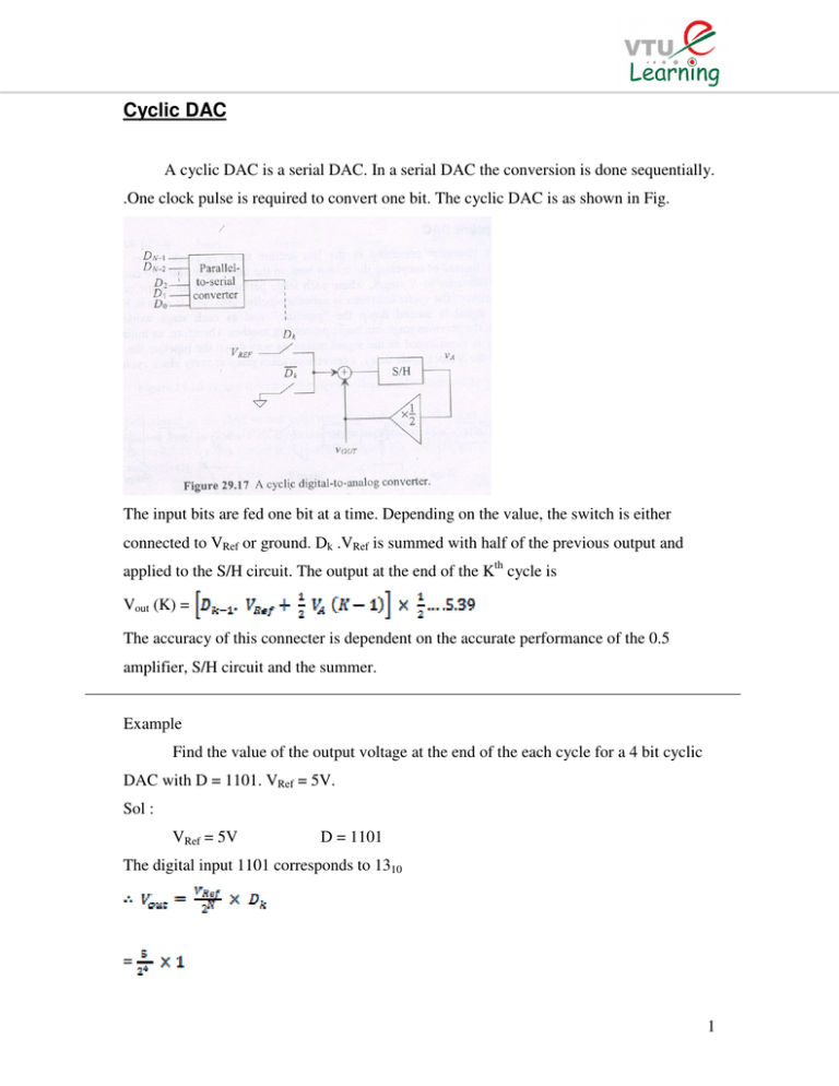
Cyclic DAC A cyclic DAC is a serial DAC. In a serial DAC the conversion is done sequentially. .One clock pulse is required to convert one bit. The cyclic DAC is as shown in Fig. The input bits are fed one bit at a time. Depending on the value, the switch is either connected to VRef or ground. Dk .VRef is summed with half of the previous output and applied to the S/H circuit. The output at the end of the Kth cycle is Vout (K) = The accuracy of this connecter is dependent on the accurate performance of the 0.5 amplifier, S/H circuit and the summer. Example Find the value of the output voltage at the end of the each cycle for a 4 bit cyclic DAC with D = 1101. VRef = 5V. Sol : VRef = 5V D = 1101 The digital input 1101 corresponds to 1310 = 1 = 4.06 V Clock cycle Vout (K) 1 1 2 0 3 1 4 1 Pipeline DAC The cyclic DAC takes N clock cycles to convert a N – bit number. Instead of feeding back the output back to the input each time, the number of stages is increased to N in the pipeline DAC. Fig 5.10 shows a 3 bit pipeline DAC. Each stage works on the conversion. If the input bit is ‘1’, VRef is added to the output of the previous stage divided by two and the value is passed to the next stage. If the input bit is ‘0’, the previous stage output is divided by two and the result is passed on. The process will become clear in example given below. 2 The signal is passed down the pipeline, as each stage works on one conversion the previous stage can begin processing another. Hence an initial N clock cycle delay is experienced as the signal moves down the pipeline. After N clock cycles conversion takes place at every clock cycle. This architecture is fast. The area occupied is N times more than the cyclic DAC. For high resolutions the amplifier gain must be accurate. Example Find the output voltage for a 3 bit pipeline DAC for inputs 001, 110 and 101 VRef = 5v. Sol : 001 Using the conventional method the output are : = 110 = 101 = Clock Vout (1) cycles 1 5x 0 0 1 2 0 2.5 x 0 0 3 5x 2.5 V 1.25 x 1 4 VOut (2) VOut 2.5 x 5 D0 D1 0 D2 0 0 1 0 1 1 The circled values pertain to the input 001 and its output 0.625V. The underlined values pertain to input 110 and its output 3.75 V. The remaining is input 101 output 3.125V. The first output is obtained at the third clock cycle. Subsequent clock cycles give the other conversions. The number of clock cycles here are five as against a cyclic DAC which would require nine clock cycles for three 3 – bit numbers. 3 ADC architectures ADC architectures are mainly of four types, Flash, Pipeline, Successive approximation and Oversampled ADCs. Here again as in DACs ADCs can be serial or parallel. Flash ADC This type of ADC shown in Fig has the highest speed. It is a parallel ADC. . Fig. illustrates a 3 bit Flash ADC. 4 The reference voltage is divided into voltage is Voltage values. At each node i the .i. The input voltage is compared with the scaled voltage and the comparator output is ‘1’ or ‘0’. The 2N – 1 : N decoder converts the input 2N – 1 bits to a N bit digital word. The area occupied by a Flash ADC on a chip doubles with each bit of increased resolution. The number of comparators is 2N -1. Apart from area power consumption by the comparators is also an issue to be considered. Although the speed is high it is limited by the switching of the comparators and the digital logic. Example For a 3 bit Flash ADC list the voltage at the nodes, the output of the comparator and the digital output VRef = 5V Sol : The voltage at the nodes can be calculated as For example V2 = = 1.25 V. V1 = 0.625 V, V2 = 1.25 V, V3 = 1.875 V, V4 = 2.5 V, V5 = 3.125 V, V6 = 3.75 V and V7 = 4.375 V Range of Vin C7 C6 C5 C4 C3 C2 C1 D0 D1 D2 0 - .625 0 0 0 0 0 0 0 0 0 0 0.625 – 1.25 0 0 0 0 0 0 1 0 0 1 1.25 – 1.875 0 0 0 0 0 1 1 0 1 0 1.875 – 2.5 0 0 0 0 1 1 1 0 1 1 2.5 – 3.125 0 0 0 1 1 1 1 1 0 0 3.125 – 3.75 0 0 1 1 1 1 1 1 0 1 3.75 – 4.375 0 1 1 1 1 1 1 1 1 0 4.375 - 5 1 1 1 1 1 1 1 1 1 1 5 Accuracy issues of Flash ADC Accuracy of the ADC is dependent on the matching of the resistor string and the input offset voltage of the comparator. Ideally the comparator should switch when V+ and V- are equal. The offset voltage of the comparator prohibits this from occurring. The comparator output V0 = 1 when V+ and V0 = 0 when V+ < V- + Vos. The switching point for the ith comparator is Vsw, i = Vi + Vos,i Where Vos i, is the offset voltage of the ith comparator. INL is given by INL = VSW, i - Vi ideal = Vi + Vos, i - Vi ideal From the resistor string DAC the voltage on the ith tap is given by equation 5.6 substituting for Vi - Vi ideal INL = The worst case INL will occur at the middle of the string i = 2N-1 then = DNL calculations can be made by using equation . The offset voltage is assumed symmetrical in both positive and negative directions. 6 Two Step flash ADC Fig. Shows the basic block diagram of a two step flash ADC. This configuration contains two complete ADCs. The first converter generates a rough estimate of the value of the input and the second ADC generates a fine tuned value. The advantage of this type of architecture is the reduction in the number of the comparators. As compared to a simple flash ADC which requires 2N-1 comparators for a two step flash ADC the number of comparators are 2 (2N/2-1) since the MSB and LSB bits are split. For example for N = 4, 2N-1 = 15 comparators and 2 (2N/2-1) = 6 comparators. The gap widens as the resolution increases. The trade off being the time taken for conversion since it takes two steps. Speed is controlled by the bandwidth and settling time required by the residue amplifier and the sub tractor. The conversion process takes two steps. In the first step the analog signal is sampled, and given to the Flash ADC which converts the MSBs. The DAC converts it back to the analog values and is given to the sub tractor. The output of 7 the subtractor is the difference between the DAC output and S / H circuit output. The residue signal is multiplied by 2N/2 and given to the second flash ADC. The second ADC produces the LSB. Some architectures use the same set of comparators in order to perform both conversions. The conversion process will become clearer from example below Example: For a 4 bit ADC give the output for analog inputs 2V, 5V, 8V, 12V. = 16V Solution: The 4 bit digital output for the analog inputs are : 2V → 0010 5V → 0101 8V → 1000 12V → 1100 The two step flash ADC consists of two 2 bit ADCs. The conversion step for the 2 bit ADC is : Input Output 0-4V 00 4-8V 01 8-12V 10 12-16V 11 For the DAC the input and output are swapped. V1=DAC Vin D3 D2 2V 00 0V 2V 8V 10 5V 01 4V 1V 4V 01 output V2 = Vin–V1 V3 = V2. 2N/2 = 4V2 D1 D0 8 8V 10 8V 0V 0V 00 12V 11 12V 0V 0V 00 Accuracy Issues: The overall accuracy of the two step flash ADC is dependent on the accuracy of the MSB ADC. The MSB ADC must have the worst care INL and DNL of that of a N-bit ADC whereas the second ADC can have the INL and DNL of that of a N/2 bit ADC. The DAC also must be equally accurate. The sub tractor and amplifier must subtract and amplify the signal to within I ½ LSB. For every bit increase in resolution the open loop gain requirement of the amplifier doubles. Linearity of the amplifier is an aspect that needs to be considered while designing an ADC. If the amplifier is not designed correctly nonlinearity is introduced. As a result of which harmonic distortion occurs, resulting in an error in the ADC. Pipeline ADC The pipeline ADC is an N. Step converter with 1 bit conversion per stage. Each stage consists of a S/H circuit, a summer and an amplifier with gain ‘2’. The configuration for a 3-bit ADC is shown in Fig.below. 9 The conversion process is as follows, the input signal is sampled and compared with by 2. If Vin < . If Vin > is passed down the pipeline after multiplying output of the comparator is ‘0’ and Vin is passed to the amplifier. The advantage of this ADC is its high throughout. Disadvantage being that is takes N clock cycles before the first digital output occurs. Also the area covered on the chip is high. The accuracy of the first stage is very crucial else the error will propagate down the pipeline. Example For a 3-bit pipeline ADC analyze the conversion process. Indicate the intermediate values. = 5V, Vin = 2V, 3. Solution : To convert the analog values directly, D= . The digital code is the equivalent of the whole number. For Vin = 2V D= = 3.2 011 3.5V D= = 5.6 101 4V D= = 6.4 110 i) For Vin = 2V Since Vin < i.e., Then V3 = 2Vin = 4V 2 < 2.5V D2 = 0 4 > 2.5V D1 = 1 10 V2 = (4 – 2.5) 2 = 3V 3> 2.5V D0 = 1 Similarly for the other inputs Vin V3 V2 D2 D1 D0 3.5V 2V 4V 1 0 1 4V 3V 1V 1 1 0 Integrating ADCs This type of ADC integrates the input signal and correlates the integration time with a digital counter. There are two types of integrating ADCs single slope and dual slope ADCs. These ADCs are used in high resolution applications but have relatively slow conversion. They are in expensive to produce. Fig illustrates a single slope ADC. 11 The single slope ADC consists of a ramp generator, an interval counter, a comparator and a counter that generates the output digital word. The input analog signal is sampled and held and given to the positive terminal of the comparator. The counters are reset. Clock is applied to both interval counter and AND gate. At the first clock pulse the ramp generator begins to integrate . If Vin is greater than the ramp voltage the output of the comparator is high. The clock pulses are passed through the AND gate and the output counter counts it. At the instant the ramp voltage becomes greater than the input voltage, as shown in Fig. , the output of the comparator goes low. The AND gate cuts off the clock pulses. The number of clock pulses passed through the AND gate (Fig. ) is counted by the output counter and the equivalent digital code is displayed. The maximum value of the input voltage is the full scale value. The counter must increment to 2N Clock cycles. This implies that the clock frequency must be many times faster than the bandwidth of the input signal. The conversion time tc is 12 Sampling rate If the analog signal bandwidth is 20 KHZ, for an 8 bit converter the clock frequency would be 2N times 2/tc or 10.24 MHZ. Any jitter in the clock will affect the overall accuracy of the ADC. The ramp generator must have a linear slope to within the accuracy of the Converter. The linearity of the ramp generator is dependent on the specifications of the opamp like open-loop gain, settling time, offset etc. Offset voltages of the S/H circuit and comparator will vary the clock pulses. There is a time delay from the time the comparator output is equal to the time the counter displays the result. The reference voltage must also stay constant for the entire period of conversion. All these points are to be considered while designing the ADC. The second type of integrating ADC is the dual slope converter. The advantage of this type of architecture is that it eliminates the dependence of the conversion process on the linearity and accuracy of the slope. A block diagram of the ADC is shown in Fig. 13 Two integrations are performed here. One on the input voltage and second on the reference voltage. The input signal is assumed to be negative since the expected slope at the output of the inverting integrator is positive. The input signal is sampled and held and integrated for a fixed interval. As is evident from the Fig. 5.15 b the slope of the input voltages for two different values is different. The integration takes place for a fixed time but the slopes are dependent on the input voltages. After the counter overflows i.e. after 2N cycles it resets. The switch is then thrown to . Since is positive the inverting integrator output will begin discharging towards zero, with a constant slope. The time taken to discharge to zero is proportional to the input voltage. From Fig. B, the slopes are different for Vin1 and Vin2. The time taken to discharge is different t1 and t2. This time t1 and t2 will be translated to the digital code. The first integration period requires 2N clock cycles. The maximum time taken for the second integration is again 2N Clock cycles. Hence the maximum time taken for conversion is 2.2N clock cycles. 14 Successive Approximation ADC The successive approximation converter performs a binary search through all possible quantization lands before converging on the final digital answer. The block diagram is shown in Fig. The N-bit shift register controls the timing of the conversion. The sampled input voltage is compared with the DAC output. The comparator output controls the direction of the binary search. The output of the SAR is the actual digital value. ‘1’ is shifted through N-bits BN-1 to B0 after each conversion. The first output of the SAR is 100…………….000, which gets converted to output of the DAC. The DAC output at each stage is compared with Vin. If at the is greater than Vin, the comparator output is ‘1’ and the comparator resets DN-1 to ‘0’. If is less than Vin, the comparator output is ‘0’ and DN-1 remains ‘1’. DN-1 is the actual MSB of the output code. Next BN-2 is set to ‘1’. DN-2 is set to ‘1’ and 15 comparison is made with or based on the value of DN-1 being ‘0’ or ‘1’ respectively. Accordingly the comparator output sets the next bit to ‘1’. The process repeats until the output of the DAC converges to the value of Vin within the resolution of the converter. Example will make the process clear. Example For the block diagram in Fig. 5.16 give the intermediate values for Vref = 8V, N=3 and Vin=3.5V, 6.5V. Sol: With Vre f = 8V it can be inferred that every rise in 1v of the input the output digital value will rise by 1. 3.5V analog will translate to 011 Cycles Vin B2 D2’D1’D0’ Vout B1 Comp D2 D1 D0 out B0 T1 3.5v 100 100 Vref/2 >Vin 1 000 T2 3.5 v 010 010 Vref/4<Vin 0 010 T3 3.5v 001 011 (1/4+1/8)Vref<Vin 0 011 T1 6.5v 100 100 Vref/2 < Vin 0 100 T2 6.5v 010 110 (1/2+1/4)Vref<Vin 0 110 T3 6.5v 001 111 (1/2+1/4+1/8)Vref>Vin 1 110 6.5V analog will translate to 110 16
